QLED and manufacturing method thereof and method for improving light extraction rate of QLED
A manufacturing method and a technology of emitting light, which are applied in semiconductor/solid-state device manufacturing, electrical components, electric solid-state devices, etc., can solve the problems of difficult application of QLED devices and high cost
- Summary
- Abstract
- Description
- Claims
- Application Information
AI Technical Summary
Problems solved by technology
Method used
Image

Examples
Embodiment 1
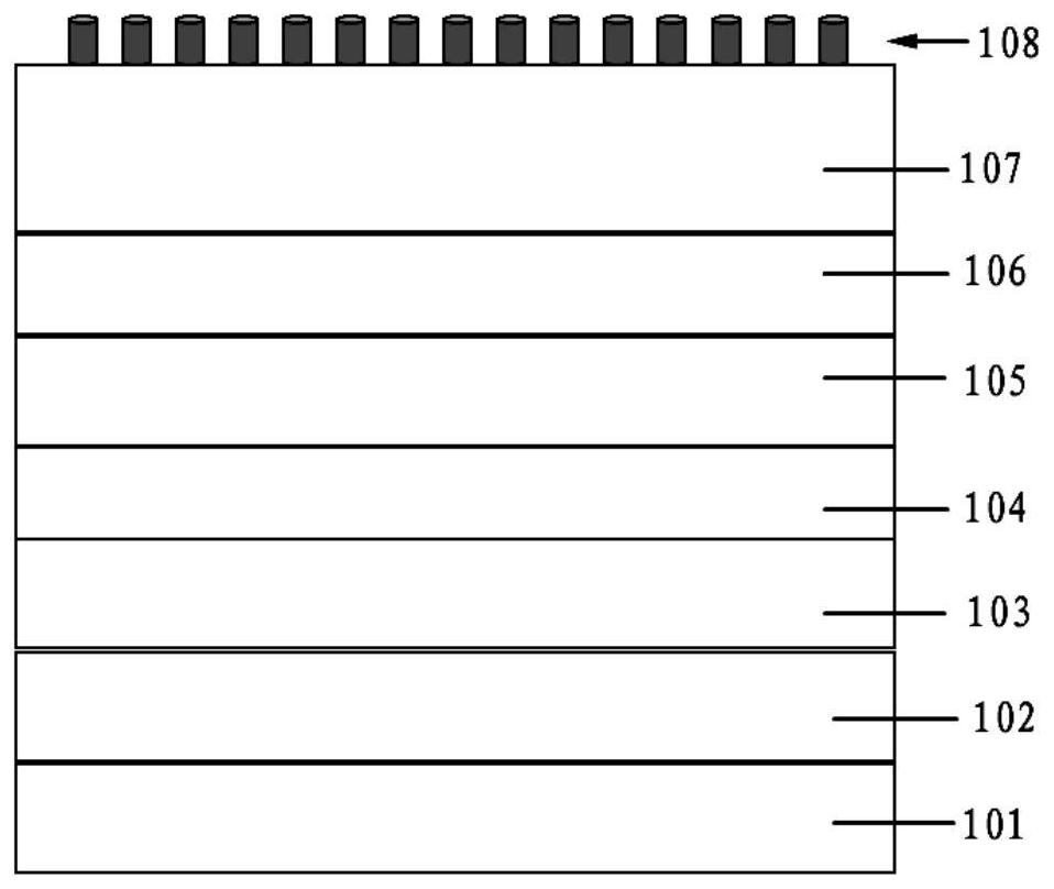
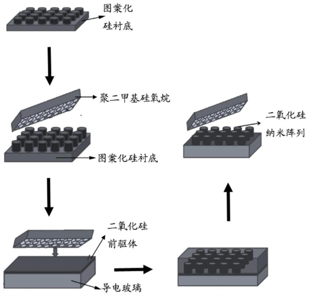
[0053] (1) Clean the silicon substrate, use the mask etching process to prepare silicon nanocolumns on the silicon substrate, the radius of the nanocolumns is 100nm, the height of the nanocolumns is 400nm, the distance between the nanocolumns (between the centers of the two nanocolumns) The distance between) is 600nm.
[0054] (2) Transfer the prepared silicon substrate to the spin coater to make it horizontal, then drop the uncured PDMS onto the surface of the silicon substrate, use 1500r / min spin coating for 20s, and then place it on a heating plate at 60 degrees Celsius After heating and curing, the PDMS is removed from the substrate for later use.
[0055] (3) Preparation of SiO by sol-gel method 2 Sol, and the sol is filtered to remove larger particles. After cleaning and drying the light-emitting surface of ITO glass, SiO 2 The sol is spin-coated onto the light-emitting surface. During spin coating, first spin coating at 500r / min for 10s, then spin coating at 4000r / m...
Embodiment 2
[0059] (1) Clean the silicon substrate, use the mask etching process to prepare silicon nanocolumns on the silicon substrate, the radius of the nanocolumns is 100nm, the height of the nanocolumns is 400nm, the distance between the nanocolumns (between the centers of the two nanocolumns) The distance between) is 600nm.
[0060] (2) Transfer the prepared silicon substrate to the spin coater to make it horizontal, then drop the uncured PDMS onto the surface of the silicon substrate, use 1750r / min spin coating for 26s, and then place it on a heating plate at 64 degrees Celsius After heating and curing, the PDMS is removed from the substrate for later use.
[0061] (3) ZnO sol was prepared by sol-gel method, and the sol was filtered to remove larger particles. After cleaning and drying the light-emitting surface of the ITO glass, spin-coat the ZnO sol onto the light-emitting surface. During spin coating, first spin coating at 630r / min for 12s, then spin coating at 4400r / min for 2...
Embodiment 3
[0065] (1) Clean the silicon substrate, use the mask etching process to prepare silicon nanocolumns on the silicon substrate, the radius of the nanocolumns is 200nm, the height of the nanocolumns is 400nm, the distance between the nanocolumns (between the centers of the two nanocolumns) The distance between) is 800nm.
[0066] (2) Transfer the prepared silicon substrate to a spin coater to make it horizontal, then drop the uncured PDMS onto the surface of the silicon substrate, spin coat it at 2000r / min for 20s, and place it on a heating plate at 76 degrees Celsius After heating and curing, the PDMS is removed from the substrate for later use.
[0067] (3) Preparation of SiO by sol-gel method 2 Sol, and the sol is filtered to remove larger particles. After cleaning and drying the light-emitting surface of ITO glass, SiO 2 The sol is spin-coated onto the light-emitting surface. During spin coating, first spin coating at 760r / min for 18s, then spin coating at 5000r / min for 3...
PUM
| Property | Measurement | Unit |
|---|---|---|
| Radius | aaaaa | aaaaa |
| Height | aaaaa | aaaaa |
| Radius | aaaaa | aaaaa |
Abstract
Description
Claims
Application Information