Jet-assisted multi-pulse-width laser peeling method for crystal ingot

An ingot and pulse width technology, applied in laser welding equipment, electrical components, circuits, etc., can solve the problems of poor processing efficiency, reduced processing efficiency, and high hardware cost, so as to improve peeling efficiency and quality, improve processing efficiency, The effect of continuous processing

Inactive Publication Date: 2020-11-06
SONGSHAN LAKE MATERIALS LAB +1
View PDF6 Cites 12 Cited by
  • Summary
  • Abstract
  • Description
  • Claims
  • Application Information

AI Technical Summary

Problems solved by technology

[0003] The publication number is CN109909627A, and the Chinese invention patent titled a laser processing equipment for SiC crystal ingots discloses a typical method of laser processing and cutting crystal ingots. Two lasers are used in the process, and the method of separate processing at two different stations not only results in high hardware costs, but also separates the processes, which increases

Method used


Image

  • Jet-assisted multi-pulse-width laser peeling method for crystal ingot
  • Jet-assisted multi-pulse-width laser peeling method for crystal ingot
  • Jet-assisted multi-pulse-width laser peeling method for crystal ingot

Examples


Embodiment 1

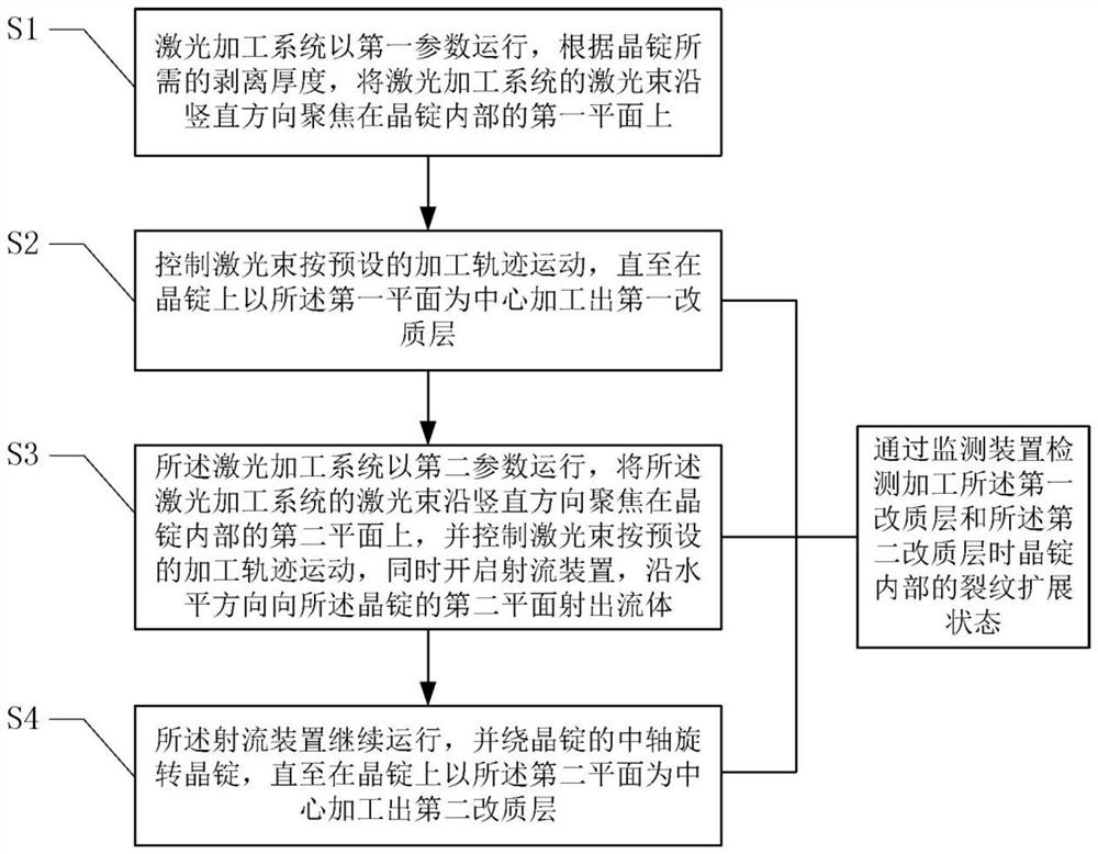
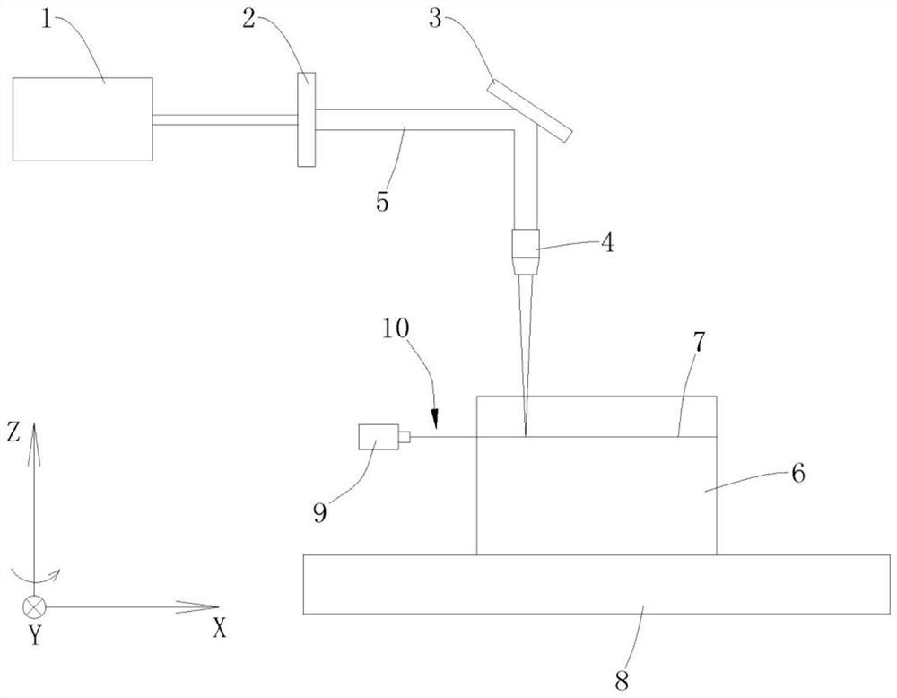
[0066] This embodiment provides a jet-assisted multi-pulse width laser crystal ingot stripping method, specifically:

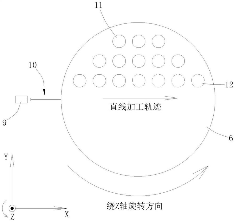
[0067] Workers or robots fix the crystal ingot 6 on the fixture of the precision motion platform 8 in advance, move the crystal ingot 6 along the X-axis and Y-axis direction, and determine the initial processing position of the crystal ingot 6 on the X-axis and Y-axis. The position is located at the edge of the crystal ingot 6, the laser processing system is set as the first parameter, the laser beam 5 of the laser processing system is focused on the first plane 500 μm away from the upper surface of the crystal ingot 6 along the vertical direction, starting from the initial processing position, Use the laser beam 5 with a pulse width of 300fs, a wavelength of 1030nm, a power of 1.5W, and a repetition rate of 100kHz to move according to the preset linear processing trajectory at a speed of 150mm / s until the laser beam 5 moves along the processing trajectory and ...

Embodiment 2

[0070] This embodiment provides a jet-assisted multi-pulse width laser crystal ingot stripping method, specifically:

[0071] Workers or robots fix the crystal ingot 6 on the fixture of the precision motion platform 8 in advance, move the crystal ingot 6 along the X-axis and Y-axis direction, and determine the initial processing position of the crystal ingot 6 on the X-axis and Y-axis. The position is located at the edge of the crystal ingot 6, the laser processing system is set as the first parameter, the laser beam 5 of the laser processing system is focused on the first plane 450 μm away from the upper surface of the crystal ingot 6 along the vertical direction, starting from the initial processing position, Use the laser beam 5 with a pulse width of 800fs, a wavelength of 1064nm, a power of 1.2W, and a repetition rate of 120kHz to move according to the preset linear processing trajectory at a speed of 130mm / s until the laser beam 5 moves along the processing trajectory and ...

Embodiment 3

[0074] This embodiment provides a jet-assisted multi-pulse width laser crystal ingot stripping method, specifically:

[0075] Workers or robots fix the crystal ingot 6 on the fixture of the precision motion platform 8 in advance, move the crystal ingot 6 along the X-axis and Y-axis direction, and determine the initial processing position of the crystal ingot 6 on the X-axis and Y-axis. The position is located at the edge of the crystal ingot 6, the laser processing system is set as the first parameter, the laser beam 5 of the laser processing system is focused on the first plane 550 μm away from the upper surface of the crystal ingot 6 along the vertical direction, starting from the initial processing position, The laser beam 5 with a pulse width of 10ps, a wavelength of 532nm, a power of 1W, and a repetition rate of 80kHz is used to process the trajectory according to the preset curve and move at a speed of 70mm / s until the laser beam 5 moves along the processing trajectory. T...


PUM

PropertyMeasurementUnit
Pulse widthaaaaaaaaaa

Abstract

The invention discloses a jet-assisted multi-pulse-width laser peeling method for a crystal ingot. The jet-assisted multi-pulse-width laser peeling method for the crystal ingot comprises the followingsteps: a laser machining system runs according to a first parameter, and a laser beam of the laser machining system is focused onto a first plane in a crystal ingot in the vertical direction; the laser beam is controlled to move according to a preset processing track until a first modified layer is machined on the crystal ingot by taking the first plane as a center; the laser machining system runs according to a second parameter, and the laser beam of the laser machining system is focused onto a second plane in the crystal ingot in the vertical direction, the laser beam is controlled to moveaccording to a preset processing track, a jet device is started simultaneously, and a fluid is jetted to the second plane of the crystal ingot in the horizontal direction; and the jet device continuesto run, and the crystal ingot is rotated around the central axis of the crystal ingot until a second modified layer is machined on the crystal ingot by taking the second plane as a center. The jet-assisted multi-pulse-width laser peeling method for the crystal ingot mainly solves the problem of dispersion of a crystal ingot peeling procedure; and the machining process is continuous, so that the machining efficiency of crystal ingot peeling is increased.

Description

technical field [0001] The invention relates to the technical field of wafer processing, in particular to a jet-assisted multi-pulse width laser crystal ingot stripping method. Background technique [0002] Ingot stripping is the main way to obtain wafers. The quality and efficiency of ingot stripping are crucial factors affecting chip manufacturing. At present, laser processing is the preferred method for ingot stripping. [0003] The publication number is CN109909627A, and the Chinese invention patent titled a laser processing equipment for SiC crystal ingots discloses a typical method of laser processing and cutting crystal ingots. Two lasers are used in the process, and the method of separate processing at two different stations not only results in high hardware costs, but also separates the processes, which increases the equipment footprint and reduces processing efficiency. [0004] The publication number is CN109834858A, and the Chinese invention patent titled peelin...

Claims


Application Information

Patent Timeline
IPC IPC(8): B23K26/38B23K26/402H01L21/301H01L21/302
CPCB23K26/38B23K26/402H01L21/30H01L21/302
Inventor 王宏建赵卫朱建海沈旋何自坚申漫漫
Owner SONGSHAN LAKE MATERIALS LAB
Why Eureka
Try Eureka