2*2 optical switch with low loss and low random phase error and N*N optical switch array

A random phase error, optical switch array technology, applied in optics, nonlinear optics, instruments, etc., can solve cumbersome problems and achieve the effects of simple process, ultra-low loss, and reduced complexity

Inactive Publication Date: 2020-11-06
ZHEJIANG UNIV
View PDF4 Cites 9 Cited by
  • Summary
  • Abstract
  • Description
  • Claims
  • Application Information

AI Technical Summary

Problems solved by technology

In order to solve this problem, it is often necessary to introduce an additional power monitor and perform very cumbersome bias calibration for each optical switch unit one by one, which makes the development of N×N optical switch arrays complicated in terms of power consumption, structure and testing. facing great challenges

Method used


Image

  • 2*2 optical switch with low loss and low random phase error and N*N optical switch array
  • 2*2 optical switch with low loss and low random phase error and N*N optical switch array
  • 2*2 optical switch with low loss and low random phase error and N*N optical switch array

Examples


specific Embodiment

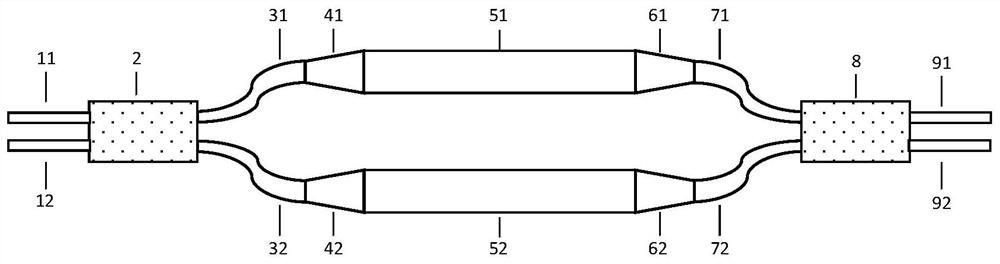
[0048] A silicon nanowire optical waveguide based on silicon-on-insulator (SOI) material is selected: its core layer is silicon material with a thickness of 220nm and a refractive index of 3.4744; its lower / upper cladding materials are all SiO 2 , the lower cladding SiO 2 Thickness of 2μm, upper cladding SiO 2 The thickness is 1 μm and the refractive index is 1.4404.

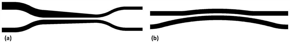
[0049] For such as figure 2 The related parameters of the curved waveguide directional coupler shown in (b) are: the width of the two curved waveguides on the inner side and the outer side are both 450nm, the distance between the two waveguides is 200nm, the bending radius of the inner waveguide is 58μm, the bending coupling angle is 21°.

[0050] For such as image 3 The Eulerian curved graded waveguide shown has the relevant parameters: the narrowest and widest waveguide widths are 450 nm and 850 nm, respectively, the maximum bending radius of the Euler curve-based curved waveguide is 25 μm, and the minim...


PUM

PropertyMeasurementUnit
thicknessaaaaaaaaaa
refractive indexaaaaaaaaaa

Abstract

The invention discloses a 2*2 optical switch with low loss and low random phase error and an N*N optical switch array. First and second input waveguides are connected with first and second front benttapered waveguides respectively after passing through a first power divider; the front bent tapered waveguides in the two groups of interference arms are sequentially connected with the rear bent tapered waveguides through the front end tapered waveguide, the phase shift waveguide and the rear end tapered waveguide; and the first rear bent tapered waveguide and the second rear bent tapered waveguide are connected with the first output waveguide and the second output waveguide through a second power divider. According to the invention, the low-loss ultra-wideband power divider is obtained in anadiabatic coupling or bending directional coupling mode; the random phase error of the interference arms is reduced by introducing the wide waveguides; and the bent tapered waveguides and the taperedwaveguides are added to further reduce the random phase error of the interference arm, so that the 2*2 optical switch with low loss and low random phase error and the N*N optical switch array are finally realized; and the optical switch has the advantages of simple structure, simple process, excellent performance and the like.

Description

technical field [0001] The invention belongs to the field of integrated optoelectronic devices, and in particular relates to a 2×2 optical switch and an N×N optical switch array with low loss and low random phase error. Background technique [0002] With the rapid development of big data, smart Internet of Things and cloud computing, the demand for ultra-large-capacity optical networks is increasing, and higher requirements are also placed on the flexibility and intelligence of the next-generation optical networks. The 2×2 optical switch is the core component of optical interconnection and optical routing. It can freely select the signal transmission channel of the integrated optical chip, which plays an important role in improving the flexibility and scalability of the optical network. Among many integrated platforms, silicon integrated devices have outstanding advantages such as small size, low power consumption, and compatibility with CMOS technology. Therefore, silicon-...

Claims


Application Information

Patent Timeline
Patent Type & Authority Applications(China)
IPC IPC(8): G02F1/225G02F1/01G02F1/035G02F1/313
CPCG02F1/0147G02F1/035G02F1/2257G02F1/3136G02F1/3138
Inventor 戴道锌刘大建宋立甲
Owner ZHEJIANG UNIV
Why Eureka
Try Eureka