Manufacturing method of Micro LED flexible circuit board

A technology of flexible circuit boards and manufacturing methods, which is applied in the manufacture of printed circuits, removal of conductive materials by chemical/electrolytic methods, printed circuits, etc., which can solve the problems of inability to guarantee quality, product deformation and shrinkage, and matrix pad line deviation To solve problems such as large tolerances, to ensure the accuracy of exposed offset, improve bonding force, and improve product quality

Active Publication Date: 2020-11-06
厦门爱谱生电子科技有限公司
View PDF5 Cites 6 Cited by
  • Summary
  • Abstract
  • Description
  • Claims
  • Application Information

AI Technical Summary

Problems solved by technology

Using the traditional manufacturing process, the deviation tolerance of the matrix pad line is large, the product deformation is large, and the ink bonding force is poor, which will make the optical performance of the product fail to meet the requirements, and the product reflection rate can only be controlled within 85%, and the reliability is poor. guaranteed quality

Method used


Image

  • Manufacturing method of Micro LED flexible circuit board
  • Manufacturing method of Micro LED flexible circuit board
  • Manufacturing method of Micro LED flexible circuit board

Examples


Embodiment Construction

[0022] The present invention will now be further described with reference to the drawings and specific embodiments.

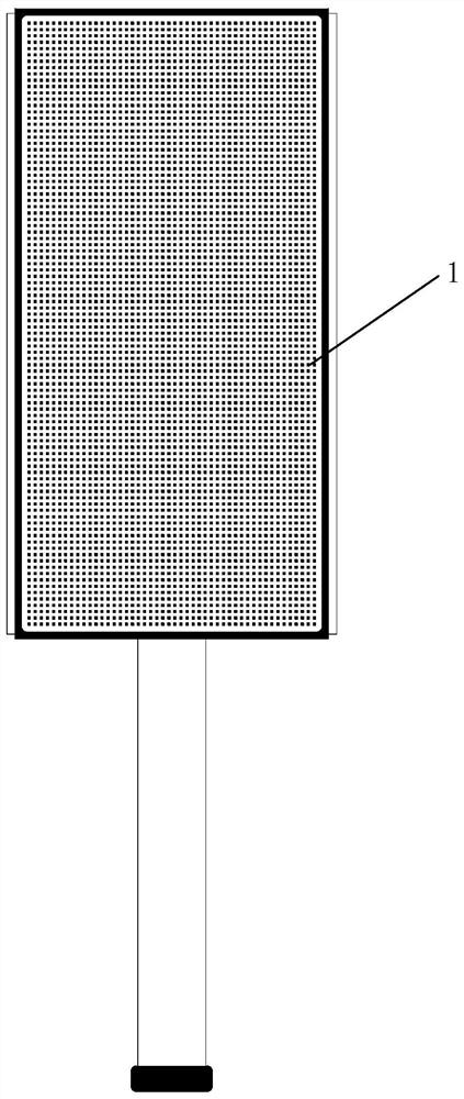
[0023] Reference figure 1 with 2 , Describes a method for manufacturing a Micro LED flexible circuit board, wherein the Micro LED flexible circuit board is a double-sided board, the main body width d1 is less than 2 mm, and the frame width d2 is less than 0.1 mm. The method includes the following steps:

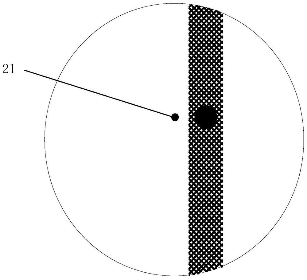
[0024] 100. Material preparation. The double-sided copper clad laminate is cut into a predetermined size, which is suitable for manufacturing a plurality of Micro LED flexible circuit board products arranged in an array. The double-sided copper clad laminate is a 1 / 3OZ halogen-free adhesive double-sided substrate. Specifically, the double-sided copper clad laminate includes a substrate layer, a white glue layer and a copper layer stacked from the inside to the outside. The thickness of the substrate layer is 13 microns, the thickness of the white glue layer is 15 ...


PUM

PropertyMeasurementUnit
diameteraaaaaaaaaa
thicknessaaaaaaaaaa
thicknessaaaaaaaaaa

Abstract

The invention relates to a manufacturing method of a Micro LED flexible circuit board. The Micro LED flexible circuit board is a double-sided board and is provided with Micro LED bonding pads distributed in a matrix mode. The method comprises the following steps: preparing materials, cutting a double-sided copper-clad plate of a preset size, and a white glue layer being arranged between a copper layer and a base material of the double-sided copper-clad plate; baking the double-sided copper-clad plate; sequentially carrying out drilling, hole blackening, plasma cleaning and copper plating; manufacturing front and back circuits; aOI, controlling the gap of the wire to be within 10% of the wire width; wherein the Micro LED bonding pad surface needs to use a white covering film, the non-MicroLED bonding pad surface uses a yellow covering film, and the white covering film corresponding to the Micro LED bonding pad region needs to be windowed; conducting punching; carrying out solder mask gold melting treatment on the bonding pad, wherein the photosensitive ink is white; sequentially carrying out reinforcing, character silk-screen printing, flying probe testing, forming, packaging and warehousing. According to the invention, the exposure offset precision of the Micro LED bonding pad can be ensured, the light reflectivity and the binding force between the photosensitive ink and a circuit are improved, and the product quality is improved.

Description

Technical field [0001] The present invention relates to the field of flexible circuit boards, in particular to a method for manufacturing a Micro LED flexible circuit board. Background technique [0002] Flexible circuit board is a kind of highly reliable and excellent flexible printed circuit board made of polyimide or polyester film as the base material, referred to as soft board or FPC, with high wiring density and light weight , Features of thin thickness. Micro LED flexible circuit board is a brand new product. Generally, each Micro LED flexible circuit board can integrate thousands of Micro LEDs, which can be applied to various display screens. Generally, such a Micro LED flexible circuit board is a double-sided board with Micro LED pads distributed in a matrix on the front side. Using traditional manufacturing technology, the matrix pad circuit has large deviation tolerances, product deformation and shrinkage, and poor ink binding force, which will make the optical perfo...

Claims


Application Information

Patent Timeline
Patent Type & Authority Applications(China)
IPC IPC(8): H05K3/00H05K3/06H05K3/28
CPCH05K3/00H05K3/0047H05K3/06H05K3/282H05K2203/052
Inventor 邹平林建华
Owner 厦门爱谱生电子科技有限公司
Why Eureka
Try Eureka