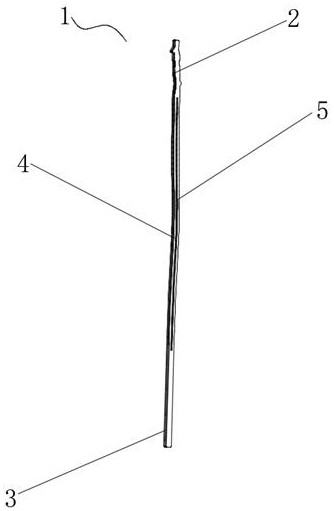
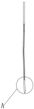
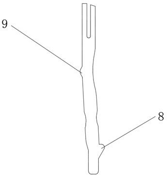
Wafer test micro probe based on micro electro mechanical system
A technology for micro-electromechanical systems and wafer testing, which is used in the testing of single semiconductor devices, components of electrical measuring instruments, and processes used to produce decorative surface effects. Chips, improve electrical conductivity, improve the effect of mechanical wear life
- Summary
- Abstract
- Description
- Claims
- Application Information
AI Technical Summary
Problems solved by technology
Method used
Image

Examples
Embodiment Construction
[0024] In the description of the present invention, it should be understood that the terms "upper", "lower", "front", "rear", "left", "right", "vertical", "horizontal", "middle", The orientation or positional relationship indicated by "内" is based on the orientation or positional relationship shown in the drawings, and is only for the convenience of describing the present invention and simplifying the description, and does not indicate or imply that the device or element referred to must have a specific orientation, It is constructed and operated in a specific orientation, so it cannot be understood as a limitation to the present invention. In addition, the terms "first", "second", etc. are only used for descriptive purposes, and cannot be understood as indicating or implying relative importance or implicitly indicating the number of indicated technical features. Thus, the features defined with "first", "second", etc. may explicitly or implicitly include one or more of these fe...
PUM
 Abstract
Description
Claims
Application Information