SOI field effect transistor capable of reducing side electric leakage and preparation method thereof

A technology of field effect transistors and main bodies, which is applied in transistors, semiconductor/solid-state device manufacturing, circuits, etc., can solve problems such as leakage and failure, and achieve the effects of reducing side leakage, increasing leakage resistance, and reducing side leakage

Active Publication Date: 2020-11-17
SHANGHAI INST OF MICROSYSTEM & INFORMATION TECH CHINESE ACAD OF SCI
View PDF4 Cites 0 Cited by
  • Summary
  • Abstract
  • Description
  • Claims
  • Application Information

AI Technical Summary

Problems solved by technology

[0003] In view of the shortcomings of the prior art described above, the purpose of the present invention is to provide a SOI field effect transistor with reduced side leakage and a preparation method thereof, which is used to solve the problem that the SOI field effect transistor has a large total dose effect in the prior art. Amplitude response causes problems such as leakage or even failure

Method used


Image

  • SOI field effect transistor capable of reducing side electric leakage and preparation method thereof
  • SOI field effect transistor capable of reducing side electric leakage and preparation method thereof
  • SOI field effect transistor capable of reducing side electric leakage and preparation method thereof

Examples


Embodiment 1

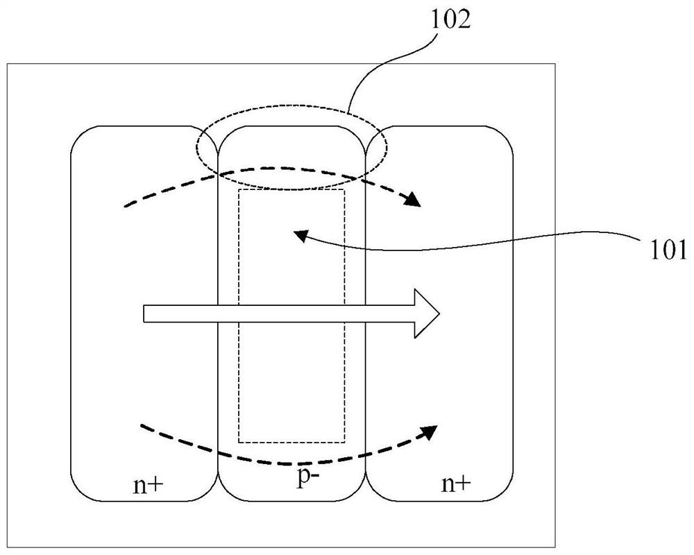
[0060] like figure 1 As shown, removing the insulating layer (BOX layer) below the channel of the SOI transistor can effectively prevent the total dose effect. This solution removes the insulating layer below the transistor channel to form a groove 101, which can effectively reduce the total dose effect. However, In the structure, the insulating layer (BOX layer) still has overlapping contact portion 102 with the conductive channel. When the total dose effect occurs, it will cause leakage in the direction of the dashed line.

[0061] Based on the above problems, such as Figure 2 to Figure 28 As shown, the present embodiment provides a method for preparing an SOI field effect transistor with reduced side leakage, and the method for preparing includes the steps of:

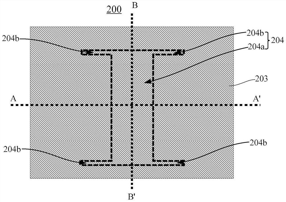
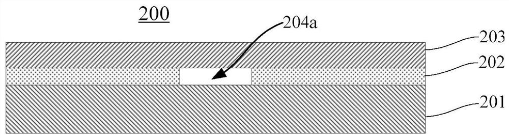
[0062] like Figure 2 to Figure 4 As shown, step 1) is first performed to provide a patterned SOI substrate 200, the patterned SOI substrate 200 includes a bottom substrate 201, an insulating layer 202 and a top...

Embodiment 2

[0088] This embodiment provides an SOI field effect transistor with reduced side leakage. The SOI field effect transistor with reduced side leakage can be prepared by the preparation method of the first embodiment above, but is not limited to the preparation method of the first embodiment, as long as it can be formed An SOI field effect transistor with reduced side leakage is sufficient. For the beneficial effect achieved by the SOI field effect transistor with reduced side leakage, please refer to Embodiment 1, which will not be repeated below.

[0089] like figure 2 , Figure 7 , Figure 25 to Figure 27 As shown, the SOI field effect transistor with reduced side leakage includes:

[0090] A patterned SOI substrate 200, the patterned SOI substrate 200 includes a bottom substrate 201, an insulating layer 202 and a top semiconductor layer 203, the insulating layer 202 below the top semiconductor layer 203 has a groove 204, the The groove 204 includes a main body groove 204...


PUM

PropertyMeasurementUnit
thicknessaaaaaaaaaa

Abstract

The invention provides an SOI (silicon on insulator) field effect transistor capable of reducing side leakage and a preparation method of the SOI field effect transistor, and the transistor comprisesa graphical SOI substrate which is provided with a bottom substrate, an insulating layer and a top semiconductor layer in the shape of a semiconductor island, wherein the insulating layer is providedwith a groove; the groove comprises a main body groove extending in the second direction and at least one expansion groove extending in the first direction, positioned at two ends of the main body groove and communicated with the main body groove; the semiconductor island completely covers the groove and comprises a first semiconductor layer extending in the first direction and a second semiconductor layer extending in the second direction, and the second semiconductor layer comprises a second main body semiconductor layer located above the main body groove and a second extended semiconductorlayer covering the extended groove; a gate structure is formed on the second semiconductor layer of the semiconductor island; and the source region and the drain region are formed at two ends of the first semiconductor layer. The expansion grooves communicated with the main body groove are formed in the two ends of the main body groove, so that the leakage resistance is effectively increased, andthe side leakage of the groove is reduced.

Description

technical field [0001] The invention belongs to the field of semiconductor design and manufacture, and in particular relates to an SOI field effect transistor with reduced side leakage and a preparation method thereof. Background technique [0002] Field effect transistors on SOI substrates have good anti-single event effects, but because in the SOI structure, the insulating layer (BOX layer) tends to accumulate more positive charges when high-energy particles are incident, the positive charges are caused in the top silicon layer of SOI. The parasitic conductive channel is created, which introduces leakage current and makes the electrical performance of the device drift. This effect is called the total dose effect, and the total dose effect is the main reason for the failure of SOI transistors in the environment of high-energy particle irradiation. Contents of the invention [0003] In view of the shortcomings of the prior art described above, the purpose of the present i...

Claims


Application Information

Patent Timeline
Patent Type & Authority Applications(China)
IPC IPC(8): H01L21/336H01L29/06H01L29/423H01L29/786
CPCH01L29/0638H01L29/0684H01L29/42376H01L29/4238H01L29/66742H01L29/78603H01L29/78609
Inventor 刘强俞文杰
Owner SHANGHAI INST OF MICROSYSTEM & INFORMATION TECH CHINESE ACAD OF SCI
Why Eureka
Try Eureka