Reflection array antenna unit, reflection array antenna and manufacturing method
A technology of reflective array antenna and manufacturing method, which is applied in the direction of antenna, antenna coupling, slot antenna, etc., can solve the problems of large antenna volume, difficulty in achieving high gain, poor signal quality, etc., achieve high gain gain, and solve electromagnetic interference and coupling Problems, High Gain Effects
- Summary
- Abstract
- Description
- Claims
- Application Information
AI Technical Summary
Problems solved by technology
Method used
Image

Examples
Embodiment 1
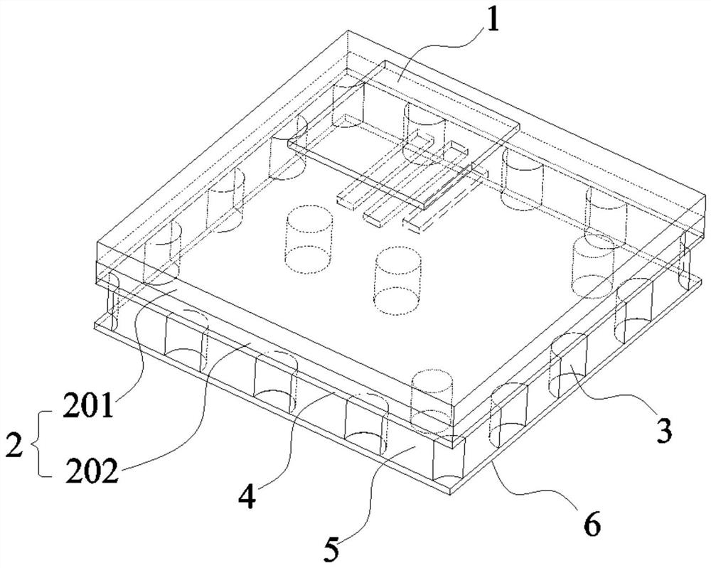
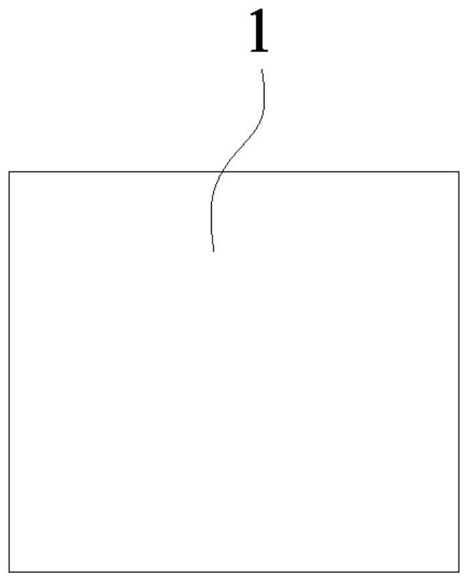
[0039] A reflectarray antenna unit, such as figure 1 and figure 2 As shown, it includes a rectangular upper dielectric substrate 2, an upper foil substrate 4, a lower dielectric substrate 5, and a lower foil substrate 6 that are sequentially connected from top to bottom; There is a radiation patch 1 at the corner of the top surface, and the upper foil plate 4 is provided with a first coupling slot 401, a second coupling slot 402, and a third coupling slot 403 located below the radiation patch 1; the lower dielectric substrate 5 contains metal Metallized via holes, together with the upper foil plate and the lower foil plate, constitute a dielectric integrated waveguide; the metallized via holes include first metallized via holes 3 evenly distributed around the antenna unit and at least one side of the radiation patch 1 .
[0040] The manufacturing method of the reflectarray antenna unit of this embodiment may include the following steps,
[0041] Bonding a radiation patch 1 a...
Embodiment 2
[0046] A reflectarray antenna unit is similar to Embodiment 1, except that the metallized via hole further includes a matching via hole 7 located at a corner of the dielectric integrated waveguide.
[0047] The above-mentioned reflectarray antenna unit may further include that at least one first metallized via hole 3 located at one end of the dielectric integrated waveguide is shifted inward to form a second metallized via hole 8 .
[0048] The above-mentioned reflectarray antenna unit may further include that the first coupling slot 401 , the second coupling slot 402 and the third coupling slot 403 are center aligned and arranged in parallel.
[0049] The above-mentioned reflectarray antenna unit may further include that the first coupling slot 401 , the second coupling slot 402 and the third coupling slot 403 are perpendicular to the propagation direction of the dielectric integrated waveguide.
[0050] The above-mentioned reflectarray antenna unit can further include that t...
Embodiment 3
[0058] A reflectarray antenna unit, similar to Embodiment 1 or Embodiment 2, the difference is that the radiation patch 1 is a square, located at the upper right corner of the top surface of the upper dielectric substrate 2, and its side length is 2 of the upper dielectric substrate 2 0.3-0.5 times the wavelength of the medium, and the thickness is 0.035mm. Such as image 3 As shown, the width of the first coupling slot 401 is 0.04-0.05 times the dielectric wavelength of the lower dielectric substrate 5 , and the length is 0.3-0.33 times the dielectric wavelength of the lower dielectric substrate 5 . The second coupling slot 402 has a width of 0.04-0.05 times the dielectric wavelength of the lower dielectric substrate 5 and a length of 0.34-0.36 times the dielectric wavelength of the lower dielectric substrate 5 . The third coupling slot 403 has a width of 0.04-0.05 times the dielectric wavelength of the lower dielectric substrate 5 and a length of 0.25-0.29 times the dielect...
PUM
| Property | Measurement | Unit |
|---|---|---|
| Thickness | aaaaa | aaaaa |
Abstract
Description
Claims
Application Information