Color film substrate and display device

A technology of color film substrate and base layer, which is applied in identification devices, nonlinear optics, optics, etc., can solve the problem that the line width cannot meet the high-resolution display device, and achieve the effect of reducing the peeling probability and improving the line width

Active Publication Date: 2020-11-20
WUHAN CHINA STAR OPTOELECTRONICS TECH CO LTD
View PDF9 Cites 0 Cited by
  • Summary
  • Abstract
  • Description
  • Claims
  • Application Information

AI Technical Summary

Problems solved by technology

[0005] The purpose of the present invention is to solve the technical problem that the line width of the existing color filter substrate cannot meet the requirements of high-resolution display devices

Method used


Image

  • Color film substrate and display device
  • Color film substrate and display device
  • Color film substrate and display device

Examples


Embodiment 1

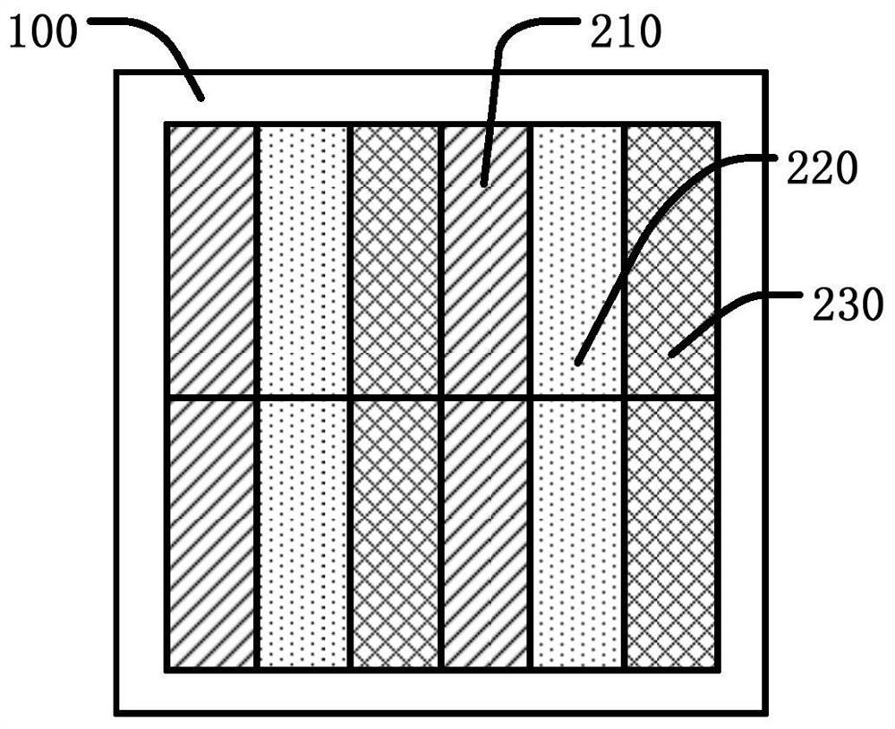
[0033] An embodiment of the present invention provides a display device, specifically including Figure 2 ~ Figure 4 As shown in the color filter substrate, the color filter substrate includes a base layer, a black matrix layer 1 and a pixel unit 2 .

[0034] The base layer acts as a substrate, and the base layer can be a flexible base layer or a hard base layer.

[0035] The black matrix layer 1 is arranged on the upper surface of the base layer, and the material of the black matrix layer 1 is a light-shielding material, which plays the role of light-shielding.

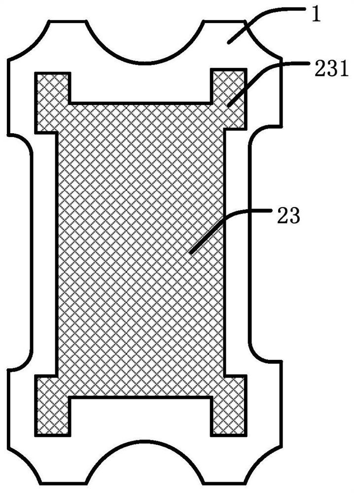
[0036] The pixel unit 2 is arranged on the upper surface of the black matrix layer 2. The pixel unit 2 includes several sub-pixels, and each sub-pixel corresponds to a color-resist layer, and the color-resist layer includes a red color-resist layer 21, a green color-resist layer 22 and a blue color-resist layer. Resistance layer 23.

[0037] An even number of pixel units 2 constitutes an arrangement period, and in ...

Embodiment 2

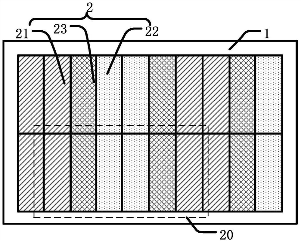
[0047] An embodiment of the present invention provides a display device, specifically including Figure 3 ~ Figure 5 As shown in the color filter substrate, the color filter substrate includes a base layer, a black matrix layer 1 and a pixel unit 2 .

[0048] The base layer acts as a substrate, and the base layer can be a flexible base layer or a hard base layer.

[0049] The black matrix layer 1 is arranged on the upper surface of the base layer, and the material of the black matrix layer 1 is a light-shielding material, which plays the role of light-shielding.

[0050] The pixel unit 2 is arranged on the upper surface of the black matrix layer 2. The pixel unit 2 includes several sub-pixels, and each sub-pixel corresponds to a color-resist layer, and the color-resist layer includes a red color-resist layer 21, a green color-resist layer 22 and a blue color-resist layer. Resistance layer 23.

[0051] An even number of pixel units 2 constitutes an arrangement period. In this...


PUM


Abstract

The invention discloses a color film substrate and a display device. The color film substrate comprises a base layer, a black matrix layer and a plurality of pixel units. Each pixel unit comprises a plurality of sub-pixels, and each sub-pixel is correspondingly provided with a color resistance layer. A plurality of even pixel units form an arrangement period and are provided with at least one pairof two adjacent pixel units, in the two adjacent pixel units, the arrangement sequence of the color resistance layers of one pixel unit is opposite to the arrangement sequence of the color resistancelayers of the other pixel unit, and in the adjacent pixel units, at least one pair of color resistance layers are the same in color. The color film substrate has the technical effects that the line width of the color film substrate is increased, and the production cost is saved.

Description

technical field [0001] The invention relates to the display field, in particular to a color filter substrate and a display device. Background technique [0002] With the improvement of display resolution requirements, for example, VR products require a resolution of 800-100ppi, which puts forward extremely high demands on the display, and the RGB line width of the color filter substrate needs to be reduced from 20-30um to 8-12um. Extremely challenging and requires the use of expensive projection exposure machines. [0003] Such as figure 1 As shown, a general color filter substrate includes a black matrix layer 100, a first color-resist layer 210, a second color-resist layer 220, and a third color-resist layer 230 are arranged sequentially on the black matrix layer 100. If this design is maintained, the RGB lines The width is 8-12um, and the process is difficult. [0004] In view of the above problems, the general countermeasures in the prior art are: to adjust the line w...

Claims


Application Information

Patent Timeline
Patent Type & Authority Applications(China)
IPC IPC(8): G09F9/30G02F1/1335
CPCG09F9/30G02F1/133512G02F1/133514
Inventor 张亦弛
Owner WUHAN CHINA STAR OPTOELECTRONICS TECH CO LTD
Why Eureka
Try Eureka