Method of forming photoresist pattern

A pattern and photoresist technology, applied in the field of forming photoresist patterns, can solve the problems of weakened light source, increased process cost, increased exposure cost, etc., and achieve the effect of small line width

Inactive Publication Date: 2003-06-04
MACRONIX INT CO LTD
View PDF0 Cites 15 Cited by
  • Summary
  • Abstract
  • Description
  • Claims
  • Application Information

AI Technical Summary

Problems solved by technology

[0004] However, there are some problems in the application of the resolution enhancement technology, such as the phase-shift mask must form a specific pattern, the fabrication of the mask is difficult and complicated, and it is not easy to modify
Off-axis illumination will weaken the light source, so it needs to provide a higher power light source, and there is still concern about the distortion of the exposure pattern
The above-mentioned problems will lead to the increase of process cost
[0005] On the other

Method used


Image

  • Method of forming photoresist pattern
  • Method of forming photoresist pattern
  • Method of forming photoresist pattern

Examples


no. 1 example

[0029] Figure 1A to Figure 1D It is a schematic flow chart of forming a photoresist pattern according to the first embodiment of the present invention.

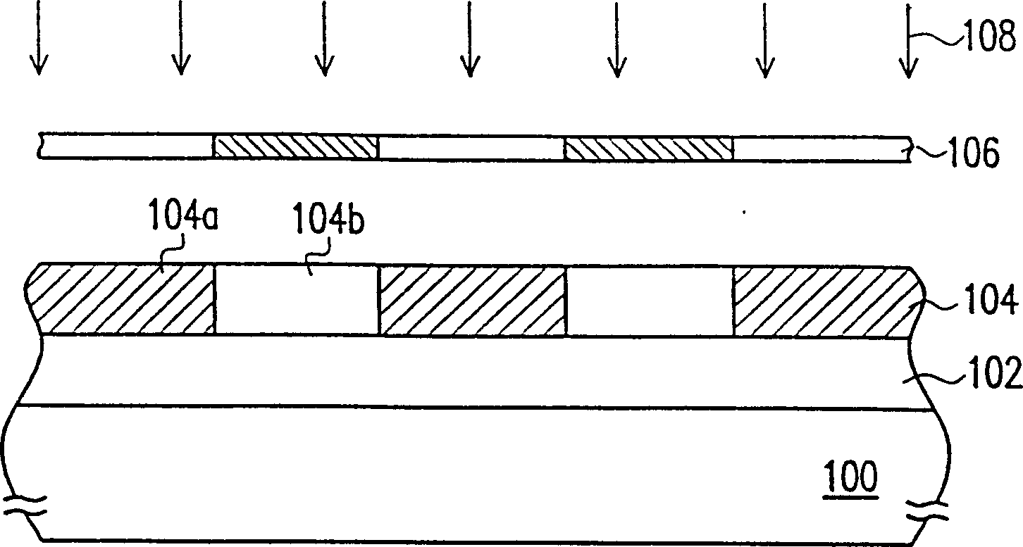
[0030] First, please refer to Figure 1A , a substrate 100 is provided, and a component structure (not shown) is formed in the substrate 100. A material layer 102 to be etched has been formed on the substrate 100. The material layer 102 to be etched is, for example, a metal layer, a polysilicon layer, a silicon nitride layer or silicon oxide layer. And a photoresist layer 104 is formed on the layer to be etched 102 , wherein the material of the photoresist layer 104 is, for example, positive photoresist.

[0031] Please continue to refer to Figure 1A , performing an exposure process 108 on the photoresist layer 104 with a photomask 106, so that the photoresist layer 104 is divided into an exposed area 104a and an unexposed area 104b. The exposed area 104 a is decomposed by light irradiation, and the unexposed area 104 b ...

no. 2 example

[0038] Figure 2A to Figure 2C It is a schematic diagram of the steps of forming a photoresist pattern according to the second embodiment of the present invention.

[0039] First, please refer to Figure 2A , first provide a substrate 200, in which a component structure (not shown) is formed, and a material layer 202 to be etched has been formed on the substrate 200, and the material layer 202 to be etched is, for example, a metal layer, a polysilicon layer, a silicon nitride layer, etc. layer or silicon oxide layer. And a photoresist layer 204 is formed on the layer to be etched 202 , wherein the material of the photoresist layer 204 is, for example, positive photoresist.

[0040] Please continue to refer to Figure 2A , performing an exposure process 208 on the photoresist layer 204 with a photomask 206, so that the photoresist layer 204 is divided into an exposed area 204a and an unexposed area 204b. The exposed area 204 a is decomposed by being irradiated with light thro...

no. 3 example

[0045] Figure 3A to Figure 3C It is a schematic flow chart of forming a photoresist pattern according to the third embodiment of the present invention.

[0046] First, please refer to Figure 3A , first provide a substrate 300, in which a component structure (not shown) is formed, and a material layer 302 to be etched has been formed on the substrate 300, and the material layer 302 to be etched is, for example, a metal layer, a polysilicon layer, a silicon nitride layer, etc. layer or silicon oxide layer. And a photoresist layer 304 is formed on the layer to be etched 302 , wherein the material of the photoresist layer 304 is, for example, negative photoresist.

[0047] Please continue to refer to Figure 3A , performing an exposure process 308 on the photoresist layer 304 with a photomask 306 , so that the photoresist layer 304 is divided into an exposed area 304 a and an unexposed area 304 b. The exposed area 304 a is irradiated with light through the light-transmitting...


PUM


Abstract

The method of forming photoresist pattern includes forming photoresist layer on the substrate, the first time exposure of the photoresist layer with mask; the first development to form the first photoresist pattern; the second time exposure of the first photoresist pattern layer to expose the decompose part of the first photoresist pattern layer and to form exposed decomposed layer; the second development to eliminate the exposed decomposed layer and to form the second positive photoresist pattern layer with pattern size smaller than that of the first photoresist pattern layer.

Description

technical field [0001] The present invention relates to a lithography process in a semiconductor process, and in particular to a method for forming a photoresist pattern capable of reducing the line width or spacing of an integrated circuit. Background technique [0002] Under the condition that circuit integration is required to be higher and higher, the design of the size of the entire circuit component is also forced to advance in the direction of continuous reduction in size. The most important process in the entire semiconductor process can be said to be the Photolithography process, which is related to the structure of Metal-Oxide-Semiconductor (MOS) components, such as: the pattern of each layer of thin film (Pattern), and The area doped with impurities (Dopants) is determined by the lithography step. In addition, whether the integration of components in the entire semiconductor industry can continue to move toward smaller line widths also depends on the development ...

Claims


Application Information

Patent Timeline
IPC IPC(8): G03F7/16G03F7/20G03F7/26
Inventor 张庆裕洪齐元
Owner MACRONIX INT CO LTD
Why Eureka
Try Eureka