Check patentability & draft patents in minutes with Patsnap Eureka AI!

Preparation method of anti-radiation GGNMOS device with block structure deep N well layer introduced

An anti-radiation, well layer technology, applied in semiconductor/solid-state device manufacturing, electric solid-state devices, semiconductor devices, etc., can solve problems such as the decline of ESD protection ability, improve the anti-single-event latch-up effect, and solve the problem of ESD trigger current overshoot. Great, improve the effect of ESD protection ability

Inactive Publication Date: 2020-11-20
58TH RES INST OF CETC
View PDF0 Cites 0 Cited by
  • Summary
  • Abstract
  • Description
  • Claims
  • Application Information

AI Technical Summary

Problems solved by technology

[0006] The object of the present invention is to provide a method for preparing a radiation-resistant GGNMOS device that introduces a deep N-well layer of a block structure, so as to solve the problem that the ESD protection ability of the existing GGNMOS device is reduced

Method used


Image

  • Preparation method of anti-radiation GGNMOS device with block structure deep N well layer introduced
  • Preparation method of anti-radiation GGNMOS device with block structure deep N well layer introduced
  • Preparation method of anti-radiation GGNMOS device with block structure deep N well layer introduced

Examples


Embodiment 1

[0057] The invention provides a method for preparing a radiation-resistant GGNMOS device that introduces a block structure deep N well layer, comprising the following steps:

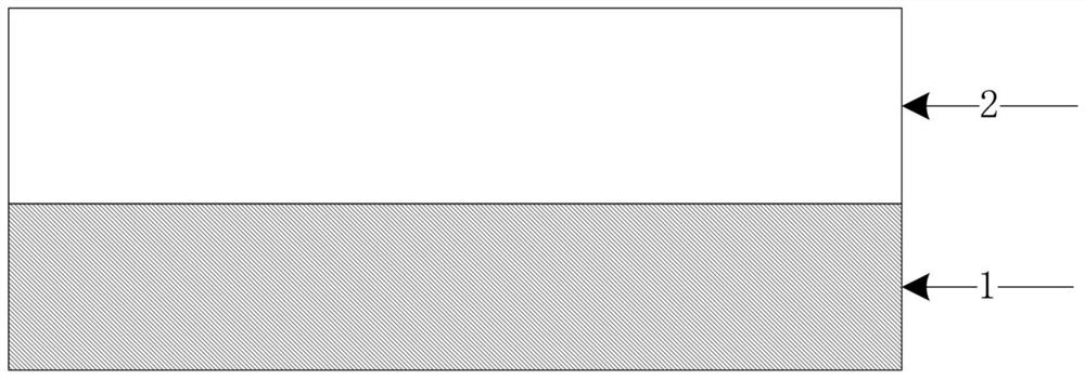
[0058] Provide an epitaxial material sheet, the epitaxial material sheet includes a P-type substrate 1 and a P-epitaxial layer 2; the thickness of the P-epitaxial layer 2 is 1.8-3.2 μm, such as figure 1 shown;

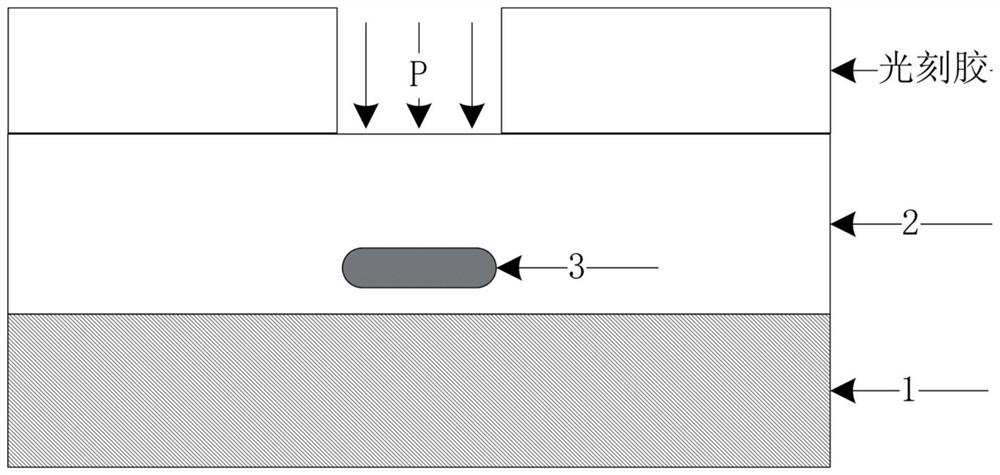
[0059] Coating photoresist on the surface of the P- epitaxial layer 2, and performing photolithography of the deep N well region of the block structure; implanting phosphorus ions through a high-energy ion implanter, and annealing to form the deep N well layer 3 of the block structure, such as figure 2 shown; the thickness of the deep N well layer 3 is 0.8 ~ 1.5 μm;

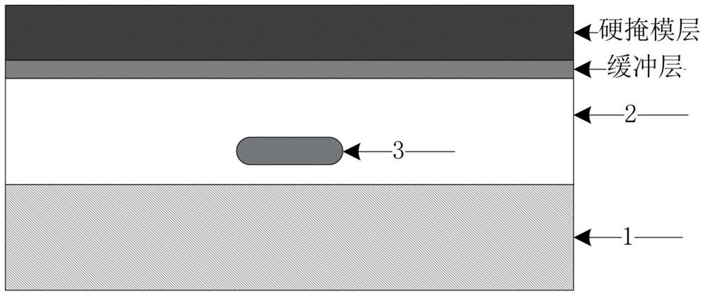
[0060] Remove the remaining photoresist, perform an oxidation on the P- epitaxial layer 2 to form a buffer layer, and then deposit silicon nitride to form a hard mask layer, such as image 3 shown;

[0061] Coating photoresist o...


PUM

PropertyMeasurementUnit
Thicknessaaaaaaaaaa
Thicknessaaaaaaaaaa

Abstract

The invention discloses a preparation method of an anti-radiation GGNMOS device with a block structure deep N well layer introduced, belongs to the technical field of electrostatic discharge protection of the integrated circuit, can be compatible with a thin epitaxial process, prepares a GGNMOS device on a P- / P+-based epitaxial substrate material, is used for the ESD protection structure of the circuit, and realizes compromise balance of single event latch resistance and ESD protection capability. By introducing the deep N well layer with the block structure, the resistance value of the body region of the GGNMOS device can be improved to a certain extent, the problem of overlarge ESD trigger current in a thin epitaxial process is solved, and the ESD protection capability is improved; and meanwhile, the P epitaxial layer and the P trap are not completely separated, so that a current discharge channel is increased, and the single event latch-up resistance of the device is improved. The preparation method of the GGNMOS device is compatible with an existing thin epitaxial process, and compromise balance of single event latch resistance and ESD protection capacity is achieved.

Description

technical field [0001] The invention relates to the technical field of electrostatic discharge protection for integrated circuits, in particular to a preparation method of a radiation-resistant GGNMOS device with a deep N well layer of a block structure. Background technique [0002] ESD is a short-term high-current discharge event, which is ubiquitous and difficult to avoid and control. It has brought great harm to the microelectronics industry. Research on ESD has become one of the important topics in the field of microelectronics today; especially Integrated circuit technology features are shrinking in size and are more susceptible to ESD damage. The current design of ESD protection structures is facing severe challenges, so it is necessary to deeply study the physical mechanism of the protection characteristics of ESD protection devices and actively take protective measures. [0003] In CMOS technology, common ESD protection devices include resistors, diodes, MOS transi...

Claims


Application Information

Patent Timeline
IPC IPC(8): H01L21/336H01L29/06H01L29/786H01L27/02
CPCH01L27/0266H01L29/0619H01L29/0684H01L29/66742H01L29/78606
Inventor 吴建伟葛超洋谢儒彬常明超张红旗
Owner 58TH RES INST OF CETC
Features
  • R&D
  • Intellectual Property
  • Life Sciences
  • Materials
  • Tech Scout
  • Unparalleled Data Quality
  • Higher Quality Content
  • 60% Fewer Hallucinations
Learn More