
Process chamber and semiconductor processing equipment

A process chamber and chamber technology, applied in semiconductor/solid-state device manufacturing, discharge tubes, electrical components, etc., can solve problems such as increasing equipment cost and structural complexity, affecting process uniformity and production capacity, and affecting the service life of parts , to achieve the effect of improving temperature control efficiency and temperature control uniformity, improving process uniformity, and increasing production capacity

Active Publication Date: 2020-11-24
BEIJING NAURA MICROELECTRONICS EQUIP CO LTD
View PDF12 Cites 4 Cited by
  • Summary
  • Abstract
  • Description
  • Claims
  • Application Information

AI Technical Summary

Problems solved by technology

[0004] However, in the prior art, since the above-mentioned heat radiation source is usually arranged at the position of the periphery of the chamber and is far away from the wafer, the heating efficiency to the wafer is low, the temperature rise rate is slow, and the heating uniformity is poor, thereby Affects process uniformity and throughput
Although the heating efficiency can be improved by increasing the power of the heat radiation source, this will have the following problems, that is, it is easy to cause the temperature of parts such as the cavity and the lining around the heat radiation source to be too high, which not only affects The service life of these parts, and additional special water-cooling design is required, which increases equipment cost and structural complexity

Method used


Image

  • Process chamber and semiconductor processing equipment
  • Process chamber and semiconductor processing equipment
  • Process chamber and semiconductor processing equipment

Examples


no. 1 example

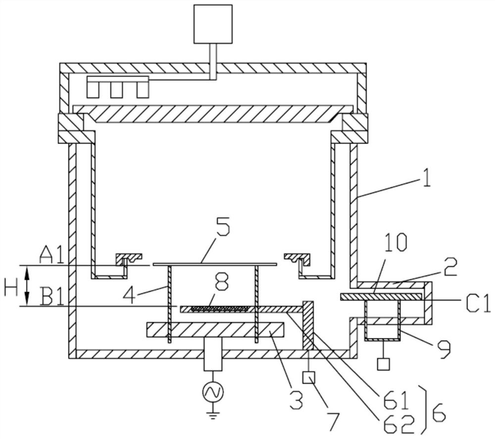
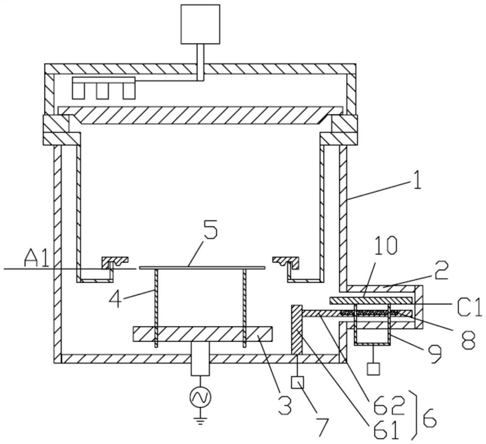
[0035] Please also refer to Figure 1A with Figure 1B , the process chamber provided in this embodiment, which can be applied to a deposition chamber, specifically includes a chamber body 1, a shielding disk library 2 communicating with the interior of the chamber body 1, a shielding disk 10 and a transmission mechanism, wherein, in The cavity main body 1 is provided with a base 3 and a first thimble mechanism 4; the base 3 is used to carry the workpiece 5 to be processed during the thin film deposition process; the first thimble mechanism 4 realizes the transfer with the base 3 by lifting Workpiece 5 to be processed. Specifically, the first thimble mechanism 4 includes at least three thimbles arranged at intervals around the axis of the base 3 and a lifting mechanism connected thereto. Driven by the lifting mechanism, the at least three thimbles can rise synchronously to a point higher than the base. The highest position of 3 or the top is lower than the lowest position of ...

no. 2 example

[0051] see Figure 4A , the present embodiment provides a process chamber, which, compared with the above-mentioned first embodiment, also includes a chamber main body 1 , a shadow disk library 2 , a shadow disk 10 and a transmission mechanism. Since the structures and functions of these components are the same as those of the above-mentioned first embodiment, they will not be repeated here, and only the differences between this embodiment and the above-mentioned first embodiment will be described in detail below.

[0052] Specifically, when the transfer arm 6 is inside the chamber main body 1 , it is located above the processed workpiece carried by the first ejector mechanism 4 . Such as Figure 4A As shown, the highest position A2 of the first ejector mechanism 4 is lower than the position B2 of the transfer arm 6 inside the chamber main body 1 . In addition, the temperature control device 8 is exposed to the lower surface of the transfer arm 6 to exchange heat with the pr...

no. 3 example

[0057] see Figure 5 , the present embodiment provides a process chamber, which, compared with the above-mentioned first and second embodiments, also includes a chamber main body 1 , a shadow disk library 2 , a shadow disk 10 and a transmission mechanism. Since the structures and functions of these components are the same as those of the above-mentioned first and second embodiments, details will not be repeated here, and only the differences between this embodiment and the above-mentioned first and second embodiments will be described in detail below.

[0058] Specifically, when the transfer arm 6 moves to the inside of the chamber main body 1 and is located at a position opposite to the workpiece 5 carried by the first ejector mechanism 4, the workpiece 5 to be processed can pass through the rising of the first ejector mechanism 4 or Move down to the position where it contacts with the transfer arm 6; and, the temperature control device 8' controls the temperature of the work...


PUM


Abstract

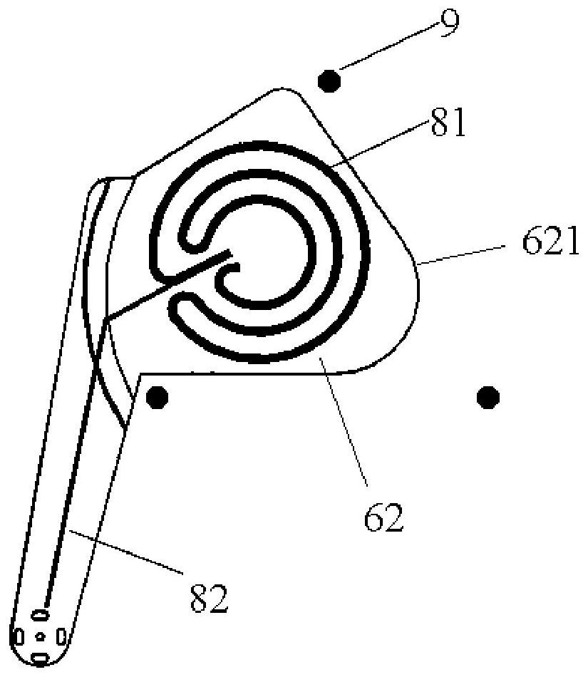
The invention provides a process chamber and semiconductor processing equipment, and the process chamber comprises a chamber main body, a shielding disc library and a shielding disc, the shielding disc library and the shielding disc are communicated with the interior of the chamber main body, and a pedestal and a first ejector pin mechanism are arranged in the chamber main body; the process chamber further comprises a transmission mechanism, the transmission mechanism comprises a transmission arm and a temperature control device, and the transmission arm can move between the cavity main body and the shielding disc library and can support the shielding disc; the temperature control device is arranged on the transmission arm and used for controlling the temperature of the machined workpiecewhen the transmission arm moves into the cavity body and is located at the position opposite to the machined workpiece borne by the first ejector pin mechanism. According to the process chamber provided by the invention, the temperature control efficiency and the temperature control uniformity can be improved, and adverse effects on other parts in the chamber are avoided.

Description

technical field [0001] The invention relates to the technical field of semiconductor processing, in particular to a process chamber and semiconductor processing equipment. Background technique [0002] In the process of using magnetron sputtering equipment for thin film deposition process, in order to save wafer consumption, when it is necessary to bombard a new target or preheat the chamber, a shielding plate is usually used to cover the top of the susceptor, while the normal During the process, the shielding disk needs to be moved into the shielding disk storage connected to the chamber. Specifically, the transfer arm is usually used to rotate to realize the position conversion of the shielding disk between the chamber main body and the shielding disk storage. [0003] In the existing copper filling process, in order to ensure that the copper material can be successfully filled in the through-hole structure, it is usually necessary to add a heat radiation source inside the...

Claims


Application Information

Patent Timeline
Patent Type & Authority Applications(China)
IPC IPC(8): H01J37/34H01L21/67
CPCH01J37/3497H01L21/67248H01J37/34H01L21/67H01J37/32H01J2237/3321
Inventor 侯珏兰玥佘清李晓强王厚工丁培军
Owner BEIJING NAURA MICROELECTRONICS EQUIP CO LTD
Learn More