Light-operated wave-absorbing active frequency selective surface

A frequency-selective surface, light-plate technology, applied in the field of electromagnetic metamaterials, can solve problems such as limited scope, no physical objects, and restrictions on electronic control components, and achieve the effect of low price and convenient use.

Active Publication Date: 2020-11-24
NANJING UNIV OF AERONAUTICS & ASTRONAUTICS
View PDF7 Cites 4 Cited by
  • Summary
  • Abstract
  • Description
  • Claims
  • Application Information

AI Technical Summary

Problems solved by technology

Commonly used photosensitive semiconductor materials include silicon, gallium arsenide, etc. There are relatively few reports on this aspect at present, and the literature only reports the simulation situation, and does not give the real object, and the semiconductor material is used as the dielectric substrate. Processing, due to the size limitation of the semiconductor wafer, this method is difficult to realize. If a cut silicon wafer is used, a large number of lasers and optical fibers are required to match it, which increases the complexity of the light feeding design and brings high design cost
There are two ways to load the light control components. One is to use photodiodes, photovoltaic cells, etc. to provide voltage to control the electronic control components. One is to directly load the photoresistor etc. into the frequency selective surface, but there is almost no research on this aspect

Method used


Image

  • Light-operated wave-absorbing active frequency selective surface
  • Light-operated wave-absorbing active frequency selective surface
  • Light-operated wave-absorbing active frequency selective surface

Examples


Embodiment Construction

[0028] Below in conjunction with accompanying drawing, technical scheme of the present invention is described in further detail:

[0029] This invention may be embodied in many different forms and should not be construed as limited to the embodiments set forth herein. Rather, these embodiments are provided so that this disclosure will be thorough and complete, and will fully convey the scope of the invention to those skilled in the art. In the drawings, components are exaggerated for clarity.

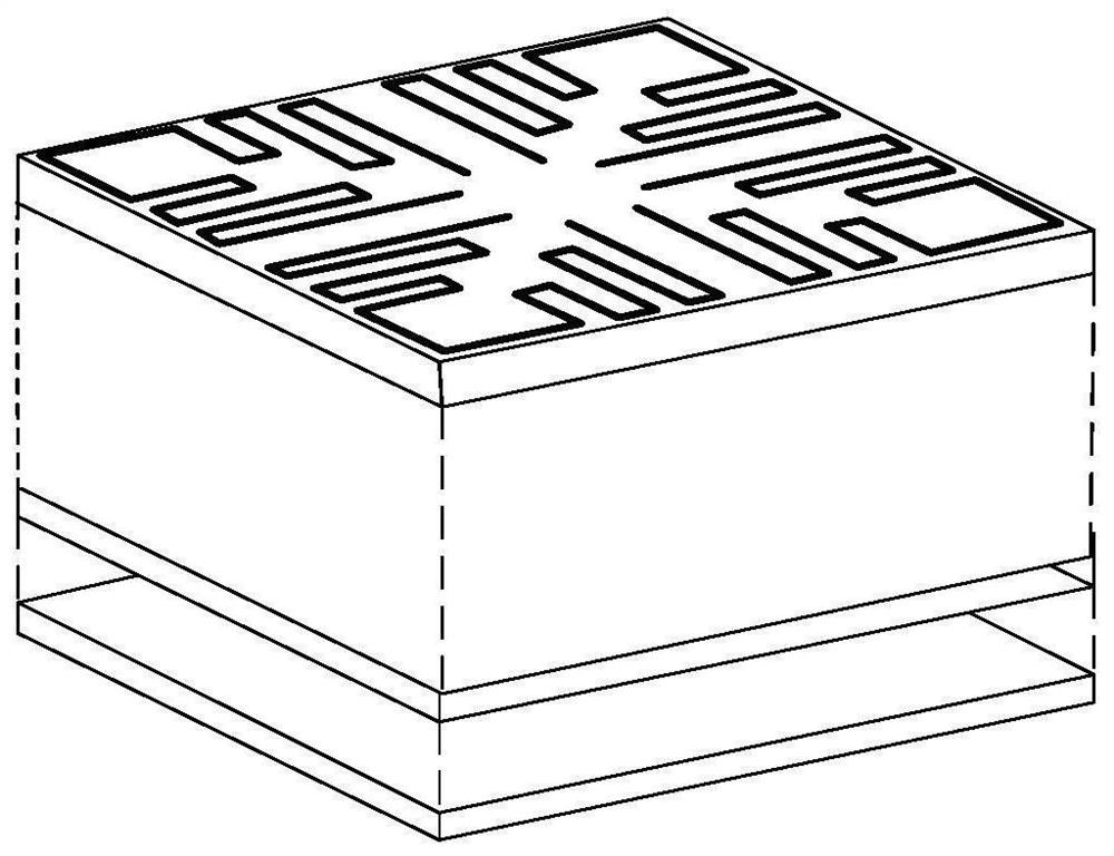
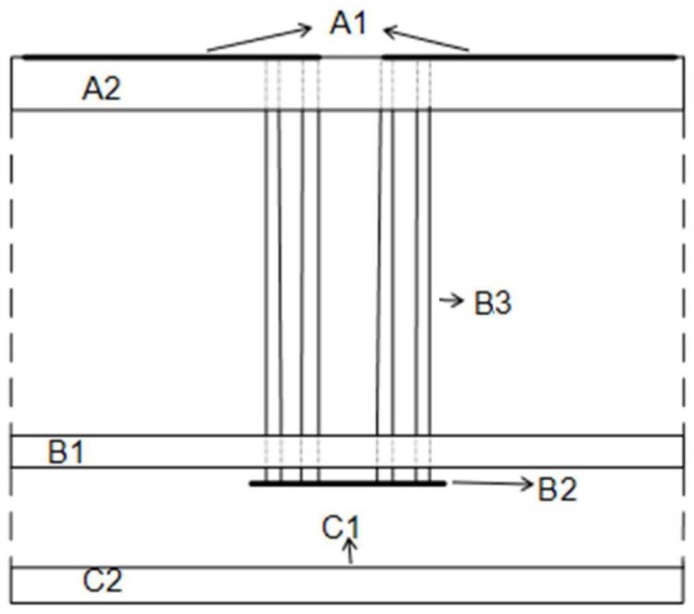
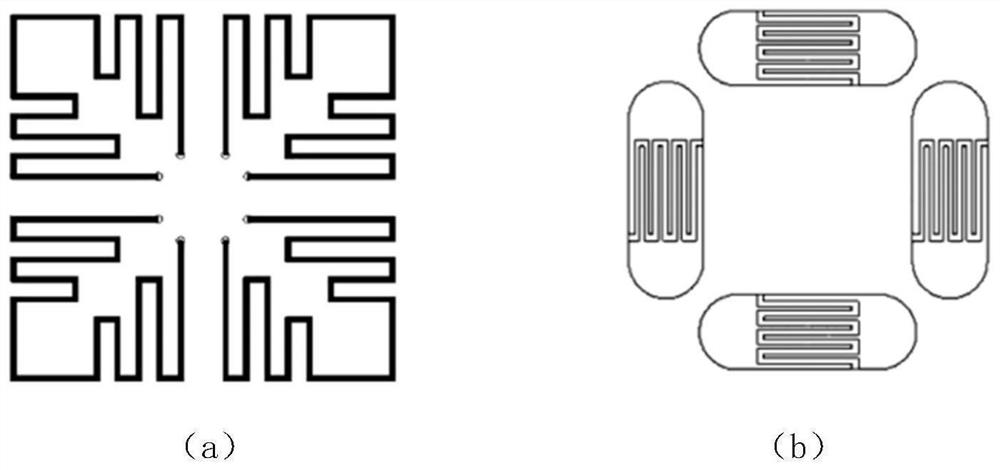
[0030] Such as figure 1 , figure 2 As shown, the present invention discloses an optically controlled wave-absorbing active frequency selective surface, comprising an upper dielectric substrate, a middle metal backplane, a lower light-feeding plate, a metal array patch, a photosensitive layer and a light-feeding layer; the upper dielectric substrate , the middle metal backplane, and the lower light-feeding plate are arranged in parallel in turn, leaving an air layer between them and ...


PUM

PropertyMeasurementUnit
thicknessaaaaaaaaaa
thicknessaaaaaaaaaa

Abstract

The invention discloses a light-operated wave-absorbing active frequency selective surface, which comprises an upper dielectric substrate, a middle metal back plate, a lower light feed plate, a metalarray patch, a photosensitive layer and a light feed layer, the metal array patch is arranged on the upper surface of the upper dielectric substrate and comprises a plurality of metal units which arearranged in a rectangular period; the photosensitive layer is arranged on the lower surface of the middle-layer metal back plate and comprises a plurality of photosensitive units in one-to-one correspondence with the metal units; and the light feeding layer is arranged on the upper surface of the lower light feeding plate and used for emitting white light with corresponding intensity to irradiatethe photosensitive surface of the photoresistor according to the magnitude of external voltage. The active control function of the frequency selective surface is realized by using a light control technology, the limitation of active lumped devices such as PIN tubes, varactors and the like on the frequency selective surface is eliminated, electromagnetic waves can be better controlled, and the frequency selective surface has important application prospects in the aspects of electromagnetic shielding, multifunctional equipment in a communication system and the like.

Description

technical field [0001] The invention relates to the technical field of electromagnetic metamaterials, in particular to an optically controlled wave-absorbing active frequency selective surface. Background technique [0002] Frequency Selective Surface (FSS) is an artificial electromagnetic material, which is composed of bending lines or gaps arranged periodically according to a certain rule. It has spatial filtering properties and can selectively transmit or shield electromagnetic waves in specific frequency bands. Divided into active FSS and passive FSS. [0003] The traditional passive FSS is a passive device. After processing, its electromagnetic performance is basically fixed, and its working performance characteristics are single. It cannot actively change its own frequency response characteristics to adapt to changes in the external electromagnetic environment, which has great limitations. Therefore, the active frequency selective surface (Active Frequency Selective S...

Claims


Application Information

Patent Timeline
Patent Type & Authority Applications(China)
IPC IPC(8): H01P1/22
CPCH01P1/222
Inventor 叶升印李黄炎曹群生王毅
Owner NANJING UNIV OF AERONAUTICS & ASTRONAUTICS
Why Eureka
Try Eureka