Tuning work function of p-metal work function films through vapor deposition

A work function, metal technology, applied in the field of semiconductor manufacturing process, can solve problems such as high resistivity

Pending Publication Date: 2020-11-24
APPLIED MATERIALS INC
View PDF1 Cites 0 Cited by
  • Summary
  • Abstract
  • Description
  • Claims
  • Application Information

AI Technical Summary

Problems solved by technology

[0003] Furthermore, the inventors have observed that although some metal nitride carbide films have a desired work function, these metal nitride carb

Method used


Image

  • Tuning work function of p-metal work function films through vapor deposition
  • Tuning work function of p-metal work function films through vapor deposition
  • Tuning work function of p-metal work function films through vapor deposition

Examples


Embodiment Construction

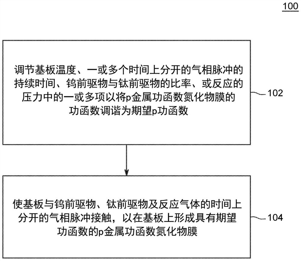
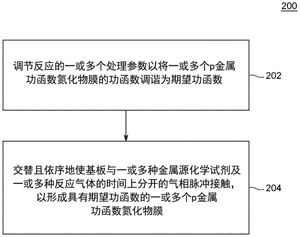
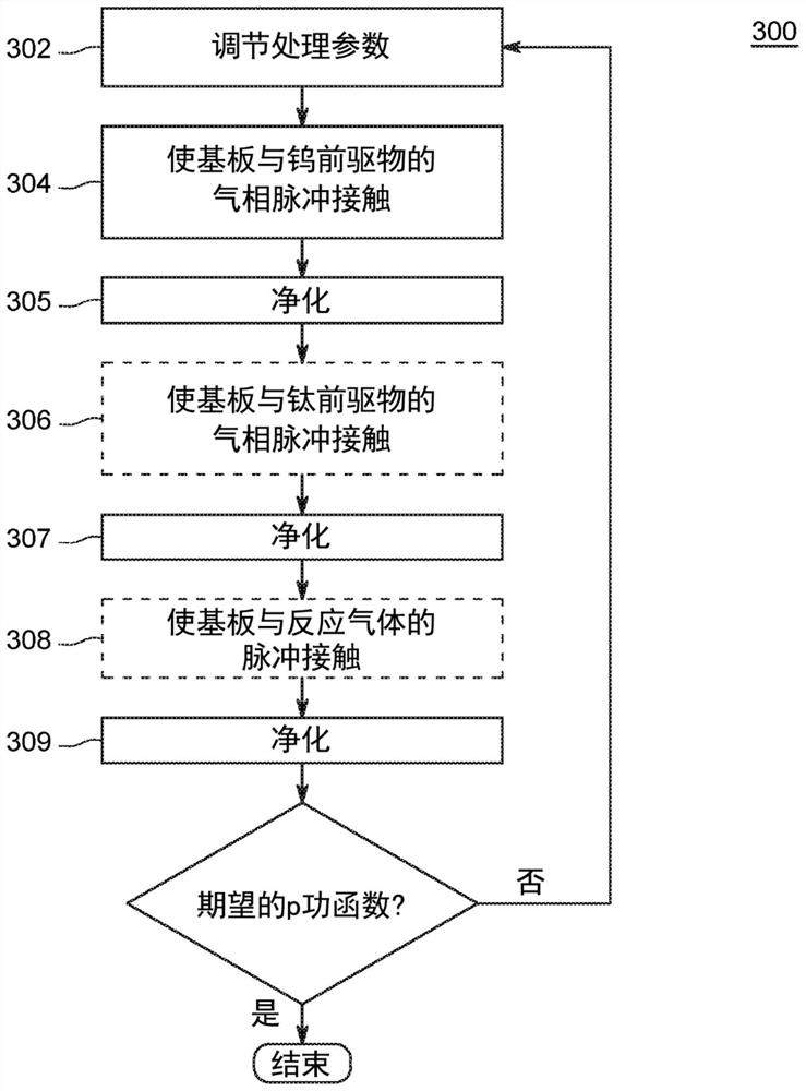
[0017] Embodiments of the present disclosure provide methods of forming one or more p-metal work function films over a substrate that advantageously tune the work function of the one or more p-metal work function nitride films. A work function tuned according to the present disclosure can be adapted to obtain a desired threshold voltage (Vt) in a semiconductor device. Accordingly, embodiments of the present disclosure may be advantageously used during different Chemical Vapor Deposition (CVD) and Atomic Layer Deposition (ALD) processes, or in devices that may undergo further processing. In some embodiments, the methods of the present disclosure advantageously provide a p-metal work function having a desired or predetermined p-work function suitable for use in Fin Field Effect Transistors (FinFETs) in the 10nm technology node and beyond. function nitride film. In an embodiment, the desired work function of the p-metal film of the present disclosure is predetermined. For examp...


PUM


Abstract

The present disclosure relates to a method for forming a p-metal work function nitride film having a desired p-work function on a substrate, including: adjusting one or more of a temperature of a substrate, a duration of one or more temporally separated vapor phase pulses, a ratio of a tungsten precursor to a titanium precursor, or a pressure of a reaction to tune a work function of a p-metal workfunction nitride film to a desired p-work function, and contacting the substrate with temporally separated vapor phase pulses of the tungsten precursor, the titanium precursor, and a reactive gas toform a p-metal work function nitride film thereon having the desired p-work function.

Description

technical field [0001] Embodiments of the present disclosure relate generally to the field of semiconductor fabrication processes and, in particular, to vapor deposition methods for work function tuning of p-metal films. Background technique [0002] Metal-oxide-semiconductor field-effect-transistor (MOSFET) such as fin field-effect transistor (finfield-effect transistor; FinFET) in 10nm technology node and other technology nodes with p metal film ), however the inventors have observed that there are still numerous challenges in this field. For example, the development of transistor technology to more advanced nodes (n < 10 nm) requires the development of low-resistivity work function metals (eg, p-metals) in transistor devices. Additionally, the threshold voltage (Vt) tuning range is greatly limited by conventional film thickness scaling due to the limited space available in the gate structure. Therefore, for work function control of p-metal films, the ability to tune ...

Claims


Application Information

Patent Timeline
IPC IPC(8): H01L21/02H01L21/324H01L29/66H01L29/78H01L21/67C23C16/455
CPCH01L21/28088H01L2029/7858H01L29/4966C23C16/45531C23C16/34H01L21/0228H01L21/324H01L29/66795H01L29/785H01L21/02205H01L21/67017H01L21/67248C23C16/45525H01L21/28506
Inventor 蹇国强唐薇林志周马伯方杨逸雄张镁刘雯伊
Owner APPLIED MATERIALS INC
Why Eureka
Try Eureka