Silicon wafer laser cutting management system and method

A laser cutting and management system technology, applied in laser welding equipment, circuits, manufacturing tools, etc., can solve the problems of low work efficiency, processing quality and yield rate, uniform thickness of single-chip silicon wafer material, and impossibility of equipment hardware precision and other issues, to achieve the effects of improving versatility and reliability, reducing processing costs and material loss, and high data transmission and processing efficiency

Inactive Publication Date: 2020-11-27
河南通用智能装备有限公司
View PDF11 Cites 1 Cited by
  • Summary
  • Abstract
  • Description
  • Claims
  • Application Information

AI Technical Summary

Problems solved by technology

[0002] At present, in the laser cutting and preparation of silicon wafers, the traditional laser cutting equipment system used can only perform single cutting or multiple cutting with a specific power and specific cutting height in a single cutting. The material thickness of a single silicon wafer itself cannot be absolutely uniform, and the hardware precision of the equipment cannot be absolutely parallel to the laser cutting point, so it is impossible to ensure that the laser focus is at an optimal position every time, resulting in cutting depth Inconsistency, so the cutting failure rate is relatively high, resulting in relatively low work efficiency, processing quality and yield of current silicon wafer laser cutting, and relatively serious material loss and relatively high processing costs

Method used


Image

  • Silicon wafer laser cutting management system and method
  • Silicon wafer laser cutting management system and method

Examples


Embodiment Construction

[0023] In order to make the technical means, creative features, goals and effects achieved by the present invention easy to understand, the present invention will be further described below in conjunction with specific embodiments.

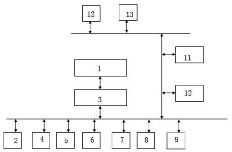
[0024] like figure 1 As shown, a silicon wafer laser cutting management system includes data operation main program 1, control interface subroutine 2, internal data communication subroutine 3, external data communication subroutine 4, data operation subroutine 5, and I / O communication Port subroutine 6, hardware driver subroutine 7, data storage subroutine 8, graphics acceleration processing subroutine 9, data detection subroutine 10 based on interrupt instruction and data detection subroutine 11 based on interrupt instruction, data operation main program 1 through Internal data communication subroutine 3 and control interface subroutine 2, external data communication subroutine 4, data operation subroutine 5, I / O communication port subroutine 6, ...


PUM


Abstract

The invention relates to a silicon wafer laser cutting management system, comprising a data running main program, a control interface subprogram, an internal data communication subprogram, an externaldata communication subprogram, a data operation subprogram, an I/O communication port subprogram, a hardware driving subprogram, a data storage subprogram, a graphic acceleration processing subprogram, a data detection subprogram based on an interrupt instruction and a data detection subprogram based on the interrupt instruction. An operation method comprises three steps of hardware system prefabrication, software system prefabrication and cutting operation. On one hand, the data storage space can be effectively saved, the requirements of data processing on a hardware system are reduced, andthe universality and the use reliability of the system are greatly improved; on the other hand, when laser cutting is carried out, the laser focus always moves along with the cutting shaft, the consistency of the laser cutting depth is ensured, and cutting errors are automatically repaired, so that the working efficiency and precision of cutting operation are greatly improved.

Description

technical field [0001] The invention relates to a silicon wafer cutting system and equipment, belonging to the field of laser microprocessing. Background technique [0002] At present, in the laser cutting and preparation of silicon wafers, the traditional laser cutting equipment system used can only perform single cutting or multiple cutting with a specific power and specific cutting height in a single cutting. The material thickness of a single silicon wafer itself cannot be absolutely uniform, and the hardware precision of the equipment cannot be absolutely parallel to the laser cutting point, so it is impossible to ensure that the laser focus is at an optimal position every time, resulting in cutting depth Inconsistency, so the failure rate of cutting is relatively high, which leads to relatively low work efficiency, processing quality and yield of current silicon wafer laser cutting, and relatively serious material loss and relatively high processing costs. [0003] Th...

Claims


Application Information

Patent Timeline
Patent Type & Authority Applications(China)
IPC IPC(8): B23K26/38B23K26/03B23K26/08B23K26/70B23K101/40
CPCB23K26/38B23K26/032B23K26/08B23K26/707B23K26/702B23K2101/40
Inventor 陶为银巩铁建蔡正道
Owner 河南通用智能装备有限公司
Why Eureka
Try Eureka