Base, device and method for epitaxial growth of silicon wafer

A technology for epitaxial growth and silicon wafers, which is applied in the directions of crystal growth, single crystal growth, single crystal growth, etc., and can solve problems such as uneven epitaxial layer thickness and poor flatness of epitaxial silicon wafers

Active Publication Date: 2020-11-27
XIAN ESWIN SILICON WAFER TECH CO LTD
View PDF7 Cites 2 Cited by
  • Summary
  • Abstract
  • Description
  • Claims
  • Application Information

AI Technical Summary

Problems solved by technology

[0008] In order to solve the above technical problems, the embodiment of the present invention expects to provide a susceptor, device and method for epitaxial growth of silicon wafers, which can solve the problems of epitaxial layer

Method used


Image

  • Base, device and method for epitaxial growth of silicon wafer
  • Base, device and method for epitaxial growth of silicon wafer
  • Base, device and method for epitaxial growth of silicon wafer

Examples


Embodiment Construction

[0033] The following will clearly and completely describe the technical solutions in the embodiments of the present invention with reference to the drawings in the embodiments of the present invention.

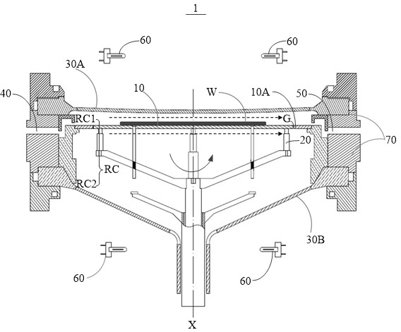
[0034] see image 3 , which shows a schematic diagram of an existing device 1 for epitaxial growth of a silicon wafer W. like image 3As shown, the device 1 may include: a base 10, which is used to carry a silicon wafer W; a base support frame 20, which is used to support the base 10 and drive the base during epitaxial growth. 10 rotates around the central axis X at a certain speed, wherein during the rotation of the base 10, the silicon wafer W rotates around the central axis X together with the base 10, that is to say, the silicon wafer W remains stationary relative to the base 10, Thus, a small gap G is required between the radial edge of the susceptor 10 and the adjacent part 10A (typically the preheating ring); the upper quartz bell 30A and the lower quartz bell 30B, th...


PUM


Abstract

The embodiment of the invention discloses a base, a device and a method for epitaxial growth of a silicon wafer, and relates to the technical field of epitaxial growth of silicon wafers. The base comprises a disc-shaped bearing part used for bearing the silicon wafer and an annular periphery extending outwards in the radial direction of the disc-shaped bearing part, wherein a plurality of throughholes are formed in the annular periphery, so that the aperture ratio of the annular periphery is gradually increased from the radial direction corresponding to the crystal orientation (100) of the silicon wafer to the radial direction corresponding to the crystal orientation (110), adjacent to the crystal orientation (100), of the silicon wafer. According to the invention, the epitaxial silicon wafer with better flatness can be obtained.

Description

technical field [0001] The invention relates to the field of epitaxial growth of silicon wafers, in particular to a base, device and method for epitaxial growth of silicon wafers. Background technique [0002] The epitaxial growth process of silicon wafers is an important process in the semiconductor chip manufacturing process. This process refers to growing a layer of crystal-free primary particles (Crystal Originated Particles, COP) defect and oxygen-free precipitated silicon single crystal layer. Epitaxial growth of silicon wafers mainly includes growth methods such as vacuum epitaxial deposition, vapor phase epitaxial deposition, and liquid phase epitaxial deposition, among which vapor phase epitaxial deposition is the most widely used. If not otherwise stated, the epitaxial growth mentioned in the present invention refers to the epitaxial growth accomplished by vapor phase epitaxial deposition. [0003] For the epitaxial growth of silicon wafers, flatness is an import...

Claims


Application Information

Patent Timeline
IPC IPC(8): C30B25/12C30B29/06
CPCC30B25/12C30B29/06
Inventor 俎世琦方圭哲金柱炫王力
Owner XIAN ESWIN SILICON WAFER TECH CO LTD
Why Eureka
Try Eureka