Miniaturized SIW resonant cavity and wide stop band SIW filter formed by same
A resonant cavity and filter technology, which is applied to waveguide-type devices, electrical components, circuits, etc., can solve the problems of large size of SIW filter and difficulty in realizing wide stop-band characteristics, and achieve the effect of compact size.
- Summary
- Abstract
- Description
- Claims
- Application Information
AI Technical Summary
Problems solved by technology
Method used
Image

Examples
Embodiment 1
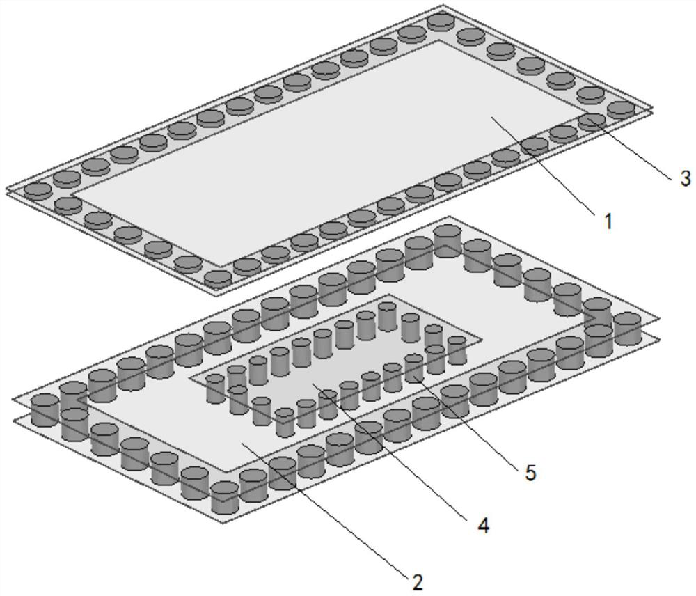
[0034] like Figure 1-3 As shown, a miniaturized SIW resonant cavity includes a top substrate 1 and a bottom substrate 2, and the top substrate 1 and the bottom substrate 2 are surrounded by first metallized via holes 3 to form electric walls to form the miniaturized SIW resonant cavity. Rectangular cavity structure;
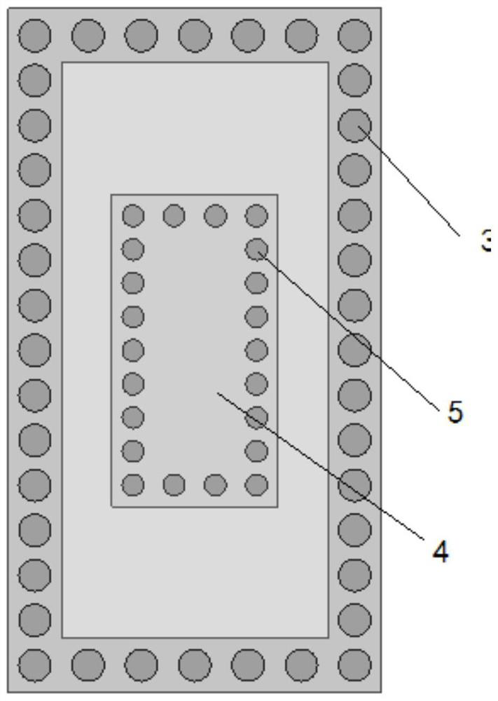
[0035] A rectangular metal patch 4 is arranged in the center of the surface of the bottom substrate 2, and a second metallized via hole 5 is arranged around the rectangular metal patch 4, and the second metallized via hole 5 is connected to the bottom substrate 2. underlying metal connections.
[0036] The miniaturized SIW resonant cavity in this embodiment adopts standard PCB processing technology, and uses a double-layer substrate to realize the recessed scheme of the bottom layer; wherein, the substrate materials of the top substrate 1 and the bottom substrate 2 are Rogers5880, the dielectric constant is 2.2, and the loss The angle tangent is 0.0009; the th...
Embodiment 2
[0039] like Figure 4-5 As shown, a wide stopband SIW filter comprising the above-mentioned miniaturized SIW resonator includes cascaded first miniaturized SIW resonator, second miniaturized SIW resonator and third miniaturized SIW resonator;
[0040] The top and bottom substrates of the first miniaturized SIW resonator, the second miniaturized SIW resonator, and the third miniaturized SIW resonator are all processed into a unified whole through PCB processing technology, and serve as the top substrate of the wide stopband SIW filter and the bottom substrate, the thicknesses of the top substrate and the bottom substrate are respectively 0.127mm and 0.508mm;
[0041] The top substrate of the above-mentioned wide stopband SIW filter is provided with an input port 6 and an output port 7; the input port 6 and the output port 7 are all made of coplanar waveguide wires with an impedance of 50 ohms, and the common The plane waveguide is connected to the first miniaturized SIW resona...
Embodiment 3
[0046] Utilize the filter structure that the present invention designs, adopt the structure parameter as shown in table 1 to carry out simulation, obtain as Figure 6 The S parameter response of the filter is shown, wherein (a) and (b) are the S parameter response curves of 5-15GHz and 5-30GHz respectively, the center frequency of the filter is set to 10GHz, and the 3dB bandwidth is 1.14GHz. It can be seen that the miniaturized filter achieves a very wide stopband bandwidth, and its high-order mode resonant frequency is 29.3GHz, achieving a suppression performance close to 3dB stopband bandwidth.
[0047] Table 1: Structure parameters of wide stopband filter for third-order miniaturization
[0048] l 1
PUM
| Property | Measurement | Unit |
|---|---|---|
| thickness | aaaaa | aaaaa |
| thickness | aaaaa | aaaaa |
| thickness | aaaaa | aaaaa |
Abstract
Description
Claims
Application Information
 - R&D
- Intellectual Property
- Life Sciences
- Materials
- Tech Scout
- Unparalleled Data Quality
- Higher Quality Content
- 60% Fewer Hallucinations
Browse by: Latest US Patents, China's latest patents, Technical Efficacy Thesaurus, Application Domain, Technology Topic, Popular Technical Reports.
© 2025 PatSnap. All rights reserved.Legal|Privacy policy|Modern Slavery Act Transparency Statement|Sitemap|About US| Contact US: help@patsnap.com