Microstrip antenna, electronic device, and OBU of ETC system
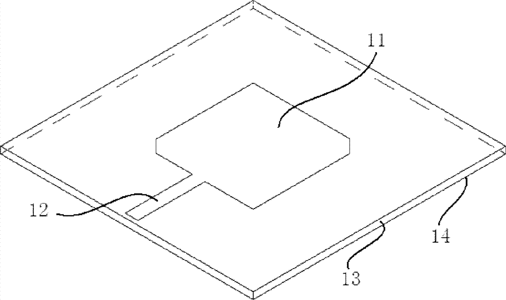
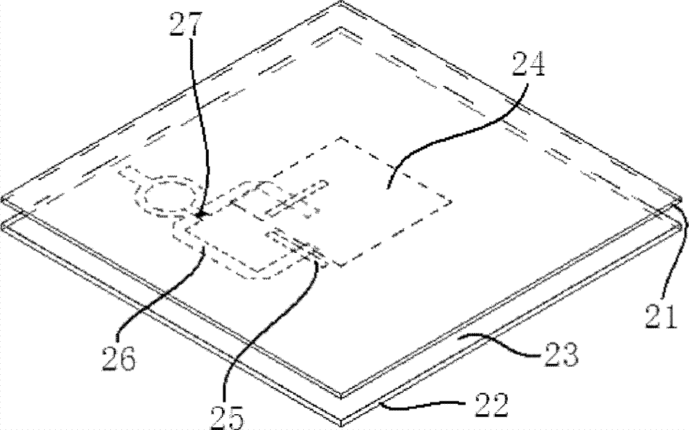
A technology of microstrip antenna and feeding network, applied in the direction of antenna, slot antenna, ticketing equipment, etc., can solve the problems of large internal space, radiating patch 24 area, large antenna volume, and occupying electronic equipment, etc., to meet the requirements of volume, The effect of saving internal space and reducing the area
- Summary
- Abstract
- Description
- Claims
- Application Information
AI Technical Summary
Problems solved by technology
Method used
Image
Examples
Embodiment 1
[0034] Such as Figure 6 to Figure 8 As shown, the microstrip antenna in this embodiment includes a first circuit board 31 and a second circuit board 32 arranged up and down and separated, both of which are PCB boards. The radiation patch 34 is a rectangular or square patch made of conductive material, and is arranged on the top or bottom surface of the first circuit board 31. The metal surface 33 can also be a rectangle or a square. The metal surface 33 and the feed network 39 are respectively arranged on The top surface and the bottom surface of the second circuit board 32, the dielectric layer is the air layer between the first circuit board 31 and the second circuit board 32, of course other dielectric layers can also be used, the structure of the microstrip antenna using the air layer is relatively simple, Easy to process. Two coupling slots 36 corresponding to the two adjacent ends of the patch slot 35 are provided on the metal surface 33 for coupling with the radiation...
Embodiment 2
[0044] An OBU of an ETC system includes the microstrip antenna described in Embodiment 1. In this example, if Figure 6 to Figure 8 As shown, the first circuit board 31 is made of FR4 board, and the second circuit board 32 is also made of FR4 board. In the design process, adopt the design method of Embodiment 2, first determine the side length of the radiation patch 34 as , then, by adjusting the size of the patch slot 35 and the auxiliary slot 35 on the radiation patch 34, and the coupling on the metal surface The size of the slot 36 enables the microstrip antenna to work stably within the prescribed working frequency band. Specifically, in this embodiment, the auxiliary slot 351 is arranged at the end of the patch slot 35 in a straight shape, and the coupling slot 36 is just located in the vertical projection area B below the radiation patch 34 . In the feed network 39, the isolation resistor of the power divider 38 is a chip resistor. The feed network 39 divides the sign...
PUM
 Abstract
Description
Claims
Application Information


