Film bulk acoustic resonator and manufacturing method thereof

A thin-film bulk acoustic wave and manufacturing method technology, applied in the direction of electrical components, impedance networks, etc., can solve the problems that cannot meet the requirements of high-performance radio frequency systems, and the quality factor of resonators cannot be further improved, so as to reduce longitudinal sound wave leakage and flatness Strong, lateral sound wave leakage improvement effect

Pending Publication Date: 2020-12-04
NINGBO SEMICON INT CORP
View PDF0 Cites 2 Cited by
  • Summary
  • Abstract
  • Description
  • Claims
  • Application Information

AI Technical Summary

Problems solved by technology

[0004] However, in the cavity-type thin-film bulk acoustic resonators produced at present, the crystal orientation of the piezoelectric layer largely depends on the electrodes below it. In order to form a better crystal orientation, t

Method used


Image

  • Film bulk acoustic resonator and manufacturing method thereof
  • Film bulk acoustic resonator and manufacturing method thereof
  • Film bulk acoustic resonator and manufacturing method thereof

Examples


Embodiment 1

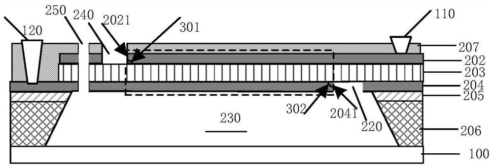
[0043] Embodiment 1 of the present invention provides a thin film bulk acoustic resonator, figure 1 It is a structural schematic diagram of the thin film bulk acoustic resonator of Embodiment 1 of the present invention, please refer to figure 1 , the thin film bulk acoustic resonator comprises:

[0044] a first substrate 100;

[0045] bonded to the support layer 206 on the first substrate 100, the support layer 206 is formed with a first cavity 230 penetrating through the support layer 206;

[0046] Piezoelectric stacked structure, covering the first cavity 230, the piezoelectric stacked structure includes sequentially stacked first electrode 202, piezoelectric layer 203 and second electrode 204 from top to bottom, in the effective resonance region ( Shown in the dashed box) the first electrode 202, the piezoelectric layer 203 and the second electrode 204 overlap in a direction perpendicular to the piezoelectric layer 203;

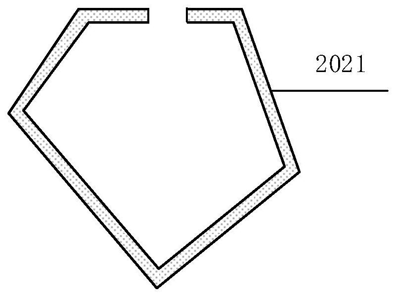
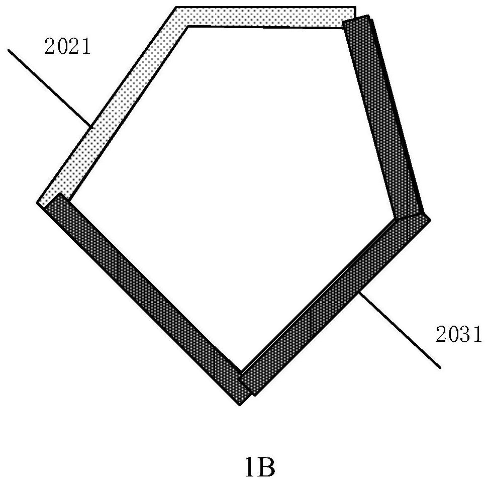
[0047] The first electrode 202 includes a first sid...

Embodiment 2

[0074] Figure 7 It is a structural schematic diagram of a thin film bulk acoustic resonator according to Embodiment 2 of the present invention.

[0075] The difference between embodiment 2 and embodiment 1 lies in that the first groove 240 and / or the second groove 220 penetrate at least a part of the thickness of the piezoelectric layer 203 . That is, the depth of the first trench 240 continues to extend down to the piezoelectric layer 203 (it may pass through the entire thickness of the piezoelectric layer 203 or end at a set depth of the piezoelectric layer 203 ) in addition to penetrating the first electrode 202 . The depth of the second trench 220 extends downwards to the piezoelectric layer 203 (it may run through the entire thickness of the piezoelectric layer 203 or may end at a predetermined depth of the piezoelectric layer 203 ) in addition to penetrating the second electrode 204 . Other structures are identical with embodiment 1, Figure 7 Only the structural diag...

Embodiment 3

[0077] Embodiment 3 of the present invention provides a method for manufacturing a thin film bulk acoustic resonator, the method comprising:

[0078] S01: providing a second substrate;

[0079] S02: forming a piezoelectric stack structure on the second substrate, the piezoelectric stack structure including a first electrode, a piezoelectric layer, and a second electrode sequentially formed on the second substrate;

[0080] S03: forming a support layer on the piezoelectric stack structure; forming a first cavity in the support layer, the first cavity passing through the support layer;

[0081] S04: providing a first substrate, bonding the first substrate on the support layer, the first substrate covering the first cavity;

[0082] S05: removing the second substrate; and

[0083] After the piezoelectric stack structure is formed, the piezoelectric stack structure is patterned to form an effective resonance area, and the boundary of the effective resonance area includes the fir...


PUM

PropertyMeasurementUnit
Angleaaaaaaaaaa
Thicknessaaaaaaaaaa
Thicknessaaaaaaaaaa

Abstract

The invention discloses a film bulk acoustic wave resonator and a manufacturing method thereof. The film bulk acoustic wave resonator comprises a first substrate; a supporting layer bonded on the first substrate, wherein a first cavity penetrating through the supporting layer is formed in the supporting layer; and a piezoelectric laminated structure covering the first cavity, wherein the piezoelectric laminated structure comprises a first electrode, a piezoelectric layer and a second electrode which are sequentially laminated from top to bottom, and the first electrode, the piezoelectric layerand the second electrode are overlapped in the direction perpendicular to the piezoelectric layer in an effective resonance area; the first electrode comprises a first side face and/or the second electrode comprises a second side face, at least part of the boundary of the effective resonance area comprises the first side face and/or the second side face, and the included angle between the first side face and/or the second side face and the surface of the piezoelectric layer is 85-95 degrees. According to the invention, the crystal orientation of the piezoelectric layer can be improved, the transverse wave loss of the resonator is reduced, and the quality factor of the film bulk acoustic resonator is improved.

Description

technical field [0001] The invention relates to the field of semiconductor device manufacturing, in particular to a thin-film bulk acoustic wave resonator and a manufacturing method thereof. Background technique [0002] Since the development of analog RF communication technology in the early 1990s, RF front-end modules have gradually become the core components of communication equipment. Among all RF front-end modules, filters have become the components with the strongest growth momentum and the greatest development prospects. With the rapid development of wireless communication technology and the maturity of 5G communication protocols, the market has also put forward stricter standards for the performance of RF filters in all aspects. The performance of a filter is determined by the resonator units that make up the filter. Among the existing filters, the film bulk acoustic resonator (FBAR) has the characteristics of small size, low insertion loss, large out-of-band suppr...

Claims


Application Information

Patent Timeline
IPC IPC(8): H03H9/02H03H9/17
CPCH03H9/02H03H9/17
Inventor 黄河罗海龙李伟
Owner NINGBO SEMICON INT CORP
Why Eureka
Try Eureka