Semiconductor package and method of forming same

A technology for semiconductors and encapsulation adhesives, applied in the fields of semiconductor devices, semiconductor/solid-state device manufacturing, electric solid-state devices, etc., can solve the problems of peeling off of packaging components, poor stability of packaging components, failure of packaging components, etc., to achieve the effect of diversifying functions

Active Publication Date: 2020-12-08
深圳伊帕思新材料科技有限公司
View PDF5 Cites 2 Cited by
  • Summary
  • Abstract
  • Description
  • Claims
  • Application Information

AI Technical Summary

Problems solved by technology

However, in the existing packaging components that combine the flexible substrate stacking structure and the POP stacking structure, it is easy to have the disadvantages of delamination of the packaging components, poor stability of the packaging components, and failure of the packaging components.

Method used


Image

  • Semiconductor package and method of forming same
  • Semiconductor package and method of forming same
  • Semiconductor package and method of forming same

Examples


Embodiment Construction

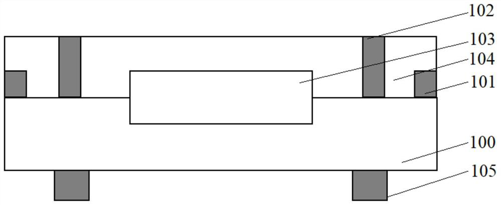
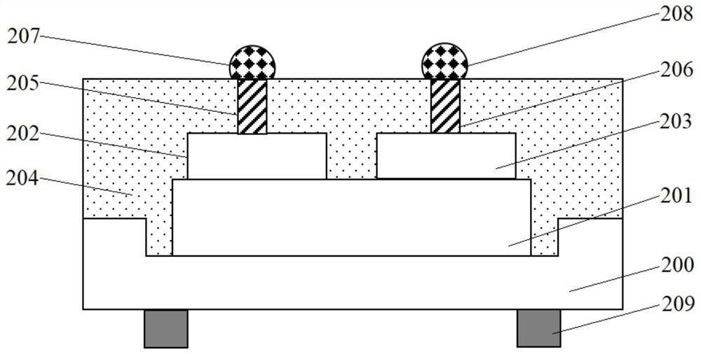
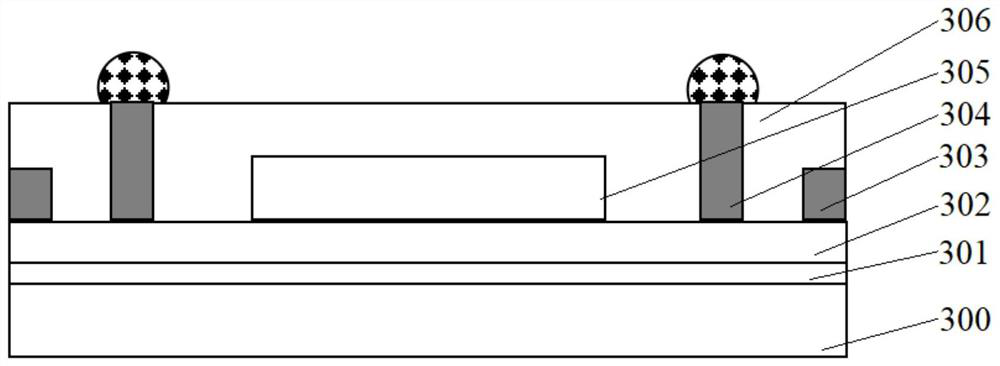
[0021] It is to be appreciated that the following disclosure provides many different embodiments, or examples, for implementing different components of the presented subject matter. Specific examples of each component and its arrangement are described below in order to simplify the description of the disclosure. Of course, these are examples only and are not intended to limit the present disclosure. For example, the following disclosure describes that a first component is formed on or over a second component, which means that it includes the embodiment in which the first component is formed in direct contact with the second component, and also includes In addition, an additional component may be formed between the first component and the second component, so that the first component may not be in direct contact with the second component. In addition, different examples in the disclosure may use repeated reference signs and / or words. These repetitions or words are used for si...


PUM


Abstract

The method comprises the following steps: forming a first packaging piece, forming second packaging pieces and forming a third packaging piece, then mounting the first packaging piece in a middle areaof a flexible circuit substrate, respectively mounting the two second packaging pieces in two opposite side edge areas of the flexible circuit substrate, forming a plurality of first through holes and second through holes which are formed at intervals, depositing a resin material in the first through holes and the second through holes to form first reinforcing columns and second reinforcing columns respectively, wherein the coefficient of thermal expansion of the resin material in the first reinforcing columns and the second reinforcing columns is smaller than the coefficient of thermal expansion of the resin material in the flexible circuit substrate, and arranging the third packaging piece on the first packaging piece, and upwards bending two opposite side edge areas of the flexible circuit substrate to enable each second packaging piece to be attached to the side wall of the first packaging piece and the side wall of the third packaging piece.

Description

technical field [0001] The invention relates to the field of semiconductor packaging, in particular to a semiconductor packaging and a forming method thereof. Background technique [0002] With people's continuous pursuit of miniaturization, systematization, and multi-function of electronic products, the feature size of VLSI is constantly shrinking. Correspondingly, the semiconductor industry has also developed rapidly. Electronic products are miniaturized and denser, with more and more functions, product sizes are getting smaller and smaller, and the distance between solder balls is getting smaller and smaller. On this basis, the POP stacking structure has also been developed rapidly. Among them, in the packaging components combined with the flexible substrate stacking structure and the POP stacking structure, chips with different functions can be stacked vertically and horizontally, thereby achieving high-density integration. , Smaller package size, superior product perfo...

Claims


Application Information

Patent Timeline
Patent Type & Authority Applications(China)
IPC IPC(8): H01L21/50H01L21/56H01L21/60H01L25/16H01L25/18
CPCH01L21/50H01L21/568H01L24/81H01L25/162H01L25/18
Inventor 孙德瑞侯新祥
Owner 深圳伊帕思新材料科技有限公司
Why Eureka
Try Eureka