
A method and device for reducing high temperature off-state leakage of semiconductor devices

A device and high-temperature technology, which is applied in the field of reducing high-temperature off-state leakage of semiconductor devices, can solve the problems of high cost and complicated process flow, and achieve the effect of low off-state leakage and reducing off-state leakage.

Active Publication Date: 2022-07-08
INST OF MICROELECTRONICS CHINESE ACAD OF SCI
View PDF7 Cites 0 Cited by
  • Summary
  • Abstract
  • Description
  • Claims
  • Application Information

AI Technical Summary

Problems solved by technology

[0005] Aiming at the problems existing in the prior art, the embodiment of the present invention provides a method and device for reducing the high-temperature off-state leakage of semiconductor devices, which is used to solve the problem of reducing the high-temperature off-state leakage of the device in the prior art, which needs to be optimized for the device structure and Substantial changes in the process flow, leading to technical problems with complex process flow and high cost

Method used


Image

  • A method and device for reducing high temperature off-state leakage of semiconductor devices
  • A method and device for reducing high temperature off-state leakage of semiconductor devices
  • A method and device for reducing high temperature off-state leakage of semiconductor devices

Examples


Embodiment 1

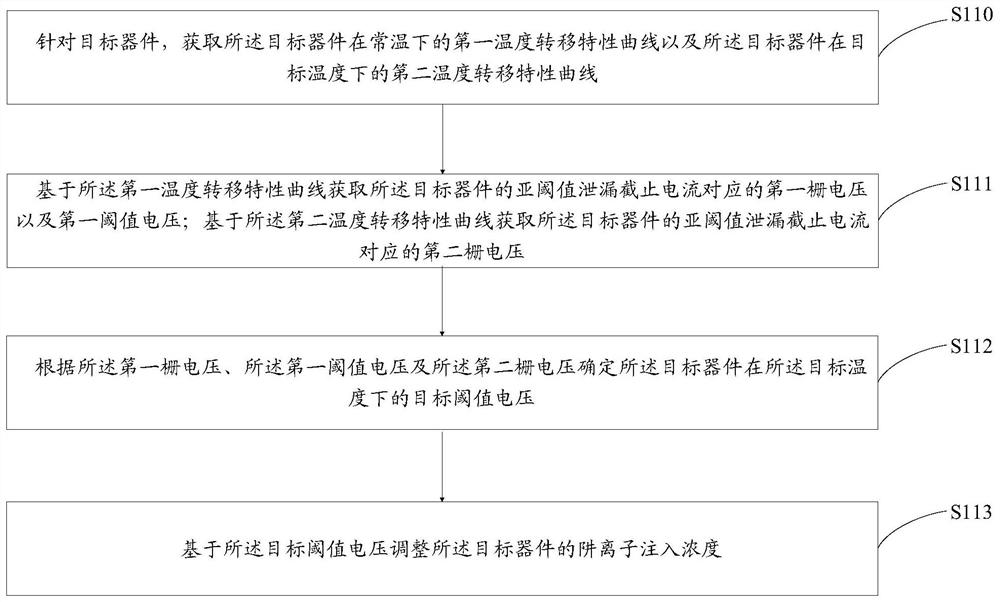
[0050] This embodiment provides a method for reducing high-temperature off-state leakage of a semiconductor device. When the temperature is greater than 125 degrees, it is called high temperature, such as figure 1 shown, methods include:

[0051] S110, for the target device, obtain a first temperature transfer characteristic curve of the target device at room temperature and a second temperature transfer characteristic curve of the target device at the target temperature;

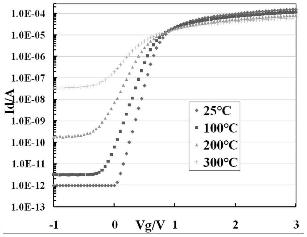
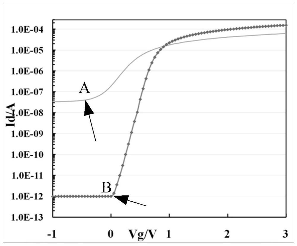
[0052] For any device, refer to figure 2 , can test the temperature transfer characteristic curve of the device at different temperatures (respectively 25°C, 100°C, 200°C and 300°C), and determine the threshold voltage (Vth), off-state leakage current of the target device from the temperature transfer characteristic curve , electrical parameters such as drive current and sub-threshold leakage cut-off current Idb. here, figure 2 It is the temperature transfer characteristic curve of NMOS device at diffe...

Embodiment 2

[0083] This embodiment provides a device for reducing high-temperature off-state leakage of a semiconductor device, such as Figure 5 As shown, the device includes: an acquisition unit 51, a determination unit 52 and an adjustment unit 53; wherein,

[0084] The obtaining unit 51 is configured to obtain, for the target device, a first temperature transfer characteristic curve of the target device at room temperature and a second temperature transfer characteristic curve of the target device at a target temperature; based on the first temperature transfer characteristic The curve obtains the first gate voltage and the first threshold voltage corresponding to the sub-threshold leakage cut-off current of the target device; the second gate voltage corresponding to the sub-threshold leakage cut-off current of the target device is obtained based on the second temperature transfer characteristic curve ;

[0085] a determining unit 52, configured to determine a target threshold voltag...


PUM


Abstract

The present invention provides a method and device for reducing high-temperature off-state leakage of a semiconductor device. The method includes: for a target device, acquiring a first temperature transfer characteristic curve of the target device at room temperature and a second temperature transfer curve of the target device at the target temperature characteristic curve; obtain the first gate voltage corresponding to the sub-threshold leakage cut-off current of the target device, the first threshold voltage and the second gate voltage corresponding to the sub-threshold leakage cut-off current; determine the target threshold voltage of the target device at the target temperature; based on the target The threshold voltage adjusts the trap ion implantation concentration of the target device; in this way, the target threshold voltage can be achieved only by implanting ions based on the adjusted ion implantation concentration; on the temperature transfer characteristic curve, it is ensured that the cutoff point of the subthreshold leakage cutoff current falls on the gate The voltage is zero, so that the off-state leakage can be minimized at the high temperature of the device without making major changes to the device structure and process flow, and the cost is guaranteed.

Description

technical field [0001] The invention belongs to the technical field of semiconductor devices, and in particular relates to a method and device for reducing high-temperature off-state leakage of semiconductor devices. Background technique [0002] Silicon-based CMOS technology is currently the mainstream technology for high-temperature integrated circuit design. However, with the reduction of threshold voltage, channel length and gate oxide thickness, high leakage current is becoming the main factor affecting high temperature CMOS circuits, resulting in increased static power consumption of high temperature integrated circuits. [0003] The main characteristics of MOS devices under high temperature conditions are the increase of leakage current and the drift of threshold voltage. Although the static power consumption of high-temperature integrated circuits can be reduced by reducing the leakage of the PN junction within the device and improving the isolation between the devi...

Claims


Application Information

Patent Timeline
Patent Type & Authority Patents(China)
IPC IPC(8): H01L21/66H01L29/06H01L21/336H01L21/265
CPCH01L29/0638H01L22/20H01L22/14H01L29/66477H01L21/265Y02P70/50
Inventor 高林春曾传滨李晓静闫薇薇倪涛李多力卜建辉张颢译王可刘海南罗家俊韩郑生
Owner INST OF MICROELECTRONICS CHINESE ACAD OF SCI
Learn More