Three-dimensional memory structure, manufacturing method thereof and three-dimensional memory device
A memory, three-dimensional technology, applied in the direction of electric solid-state devices, semiconductor devices, electrical components, etc., can solve problems such as uneven stress distribution, low storage capacity, unstable structure of three-dimensional memory devices, etc., to achieve improved stability and uniform stress distribution Effect
- Summary
- Abstract
- Description
- Claims
- Application Information
AI Technical Summary
Problems solved by technology
Method used
Image

Examples
Embodiment 1
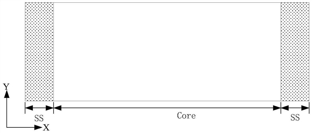
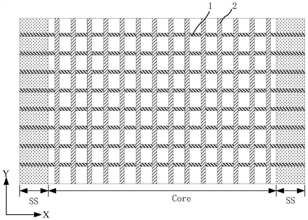
[0068] Figure 7 A top view of the three-dimensional memory structure 100 of this embodiment is shown, Figure 8 shown in Figure 7 The top view of the three-dimensional memory structure 100 after forming the gate spacer 1 and the bit line 2, please refer to Figure 7 , the three-dimensional memory structure 100 includes a substrate (not shown) and a stack structure, and the stack structure is formed on the substrate.
[0069] In this embodiment, the three-dimensional memory structure 100 includes a substrate at the bottom, such as a semiconductor substrate, the substrate can be selected according to the actual requirements of the device, and the substrate can include a silicon substrate , germanium (Ge) substrate, silicon germanium (SiGe) substrate, SOI (Silicon-on-insulator, silicon-on-insulator) substrate or GOI (Germanium-on-Insulator, germanium-on-insulator) substrate, etc., in In other embodiments, the substrate can also be a substrate including other elemental semico...
Embodiment 2
[0078] Figure 9 A top view of the three-dimensional memory structure 200 of this embodiment is shown, Figure 10 shown in Figure 9 The top view of the three-dimensional memory structure 200 after forming the gate spacer 1 and the bit line 2, please refer to Figure 9 and Figure 10 , the three-dimensional memory structure 200 includes a substrate (not shown) and a stack structure, and the stack structure is formed on the substrate. The difference between the present embodiment and the first embodiment is that a gate wall structure 3 is provided in the step area of each partition, and other structures are the same as those of the first embodiment, so repeated descriptions will not be repeated. see Figure 9 , the gate wall structure 3 extends from an end of the step area away from the core array area to an end close to the core array area, and the gate wall structure 3 is a partial stack that is completely preserved during the process of forming steps by an etching trim...
Embodiment 3
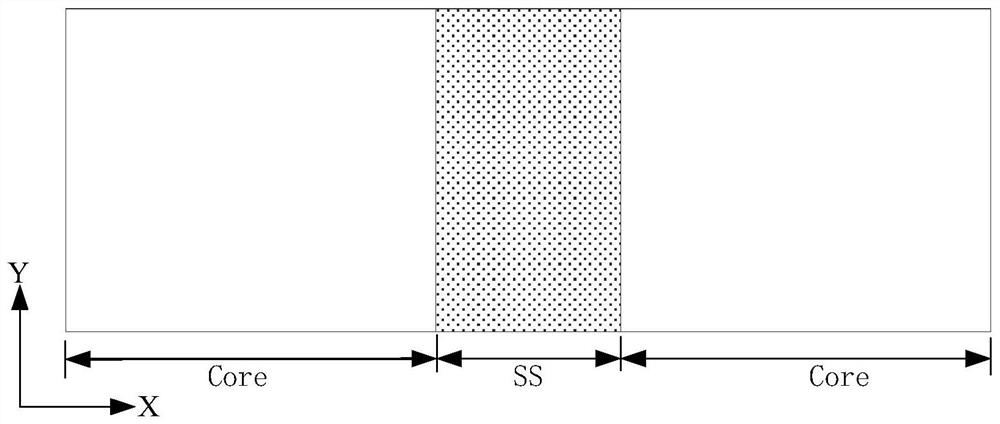
[0081] Figure 11 A top view of the three-dimensional memory structure 300 of this embodiment is shown, Figure 12 shown in Figure 11 For the top view of the three-dimensional memory structure 300 in which the gate spacer 1 and the bit line 2 are formed, please refer to Figure 11 , the three-dimensional memory structure 300 includes a substrate (not shown) and a stack structure, and the stack structure is formed on the substrate. The difference between the present embodiment and the first embodiment lies in that the relative positions of the step area and the core array area in each subregion are different, and other structures are the same as those of the first embodiment, so no repeated description is given. see Figure 11 , in this embodiment, the first stepped area S1 is arranged on the side (lower side) of the first subregion A1 close to the third subregion A3; the second stepped region S2 is arranged on the second subregion A3 The side (left side) of the second sub...
PUM
 Abstract
Description
Claims
Application Information
 - R&D
- Intellectual Property
- Life Sciences
- Materials
- Tech Scout
- Unparalleled Data Quality
- Higher Quality Content
- 60% Fewer Hallucinations
Browse by: Latest US Patents, China's latest patents, Technical Efficacy Thesaurus, Application Domain, Technology Topic, Popular Technical Reports.
© 2025 PatSnap. All rights reserved.Legal|Privacy policy|Modern Slavery Act Transparency Statement|Sitemap|About US| Contact US: help@patsnap.com