

Method for determining wafer processing parameters and wafer processing method
A technology of processing parameters and processing procedures, which is applied in the field of determining wafer processing parameters and wafer processing, and can solve the problems that the notch line cannot represent the cutting condition, the process personnel cannot trace and control, and the wafer process cannot be known.
- Summary
- Abstract
- Description
- Claims
- Application Information
AI Technical Summary
Problems solved by technology
Method used
Image

Examples
Embodiment Construction
[0027] Embodiments of the present invention are described in detail below. The embodiments described below are exemplary only for explaining the present invention and should not be construed as limiting the present invention. If no specific technique or condition is indicated in the examples, it shall be carried out according to the technique or condition described in the literature in this field or according to the product specification. The reagents or instruments used were not indicated by the manufacturer, and they were all commercially available conventional products.
[0028] In one aspect of the invention, the invention provides a method of determining wafer processing parameters.
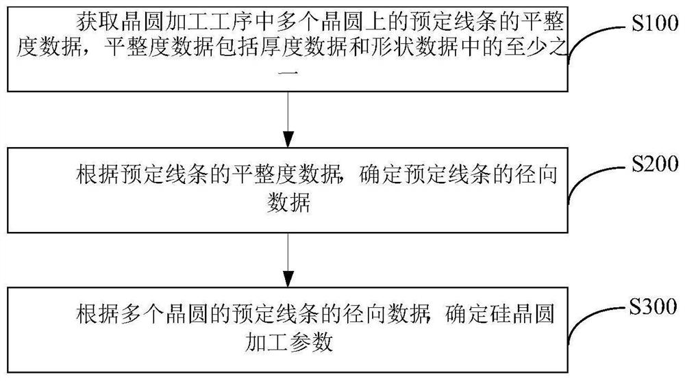
[0029] According to an embodiment of the present invention, refer to figure 1 , the method for determining wafer processing parameters comprises the following steps:
[0030] S100: Obtain flatness data of predetermined lines on a plurality of wafers in a wafer processing procedure, where...
PUM
 Abstract
Description
Claims
Application Information