Efficient drilling method for multi-layer PCB

A technology of PCB board and drilling method, which is applied in the field of high-efficiency drilling of multi-layer PCB boards, can solve the problems of reducing the drilling speed of PCB boards, drilling deviation of debris PCB boards, and inconvenient processing for users, so as to avoid PCB board drilling The effect of hole deviation, increasing the thickness of PCB board, and facilitating processing

Inactive Publication Date: 2020-12-15
深圳市联创电路有限公司
View PDF0 Cites 1 Cited by
  • Summary
  • Abstract
  • Description
  • Claims
  • Application Information

AI Technical Summary

Problems solved by technology

[0002] The Chinese name of the PCB board is a printed circuit board, also known as a printed circuit board. It is an important electronic component, a support for electronic components, and a carrier for the electrical connection of electronic components; because it is made by electronic printing, so It is called a printed circuit board; the traditional PCB board is directly drilled with a drill bit, and the processing is prone to deviation, which reduces the drilling speed of the PCB board, resulting in extremely inefficient drilling, and time-consuming and laborious, and debris is easy to accumulate and cause PCB board drilling. Hole deviation, and there is no solution according to different processing problems, which is inconvenient for users to process; in view of these defects, it is necessary to design an efficient drilling method for multi-layer PCB boards

Method used


Image

  • Efficient drilling method for multi-layer PCB

Examples


Embodiment Construction

[0031] The following will clearly and completely describe the technical solutions in the embodiments of the present invention with reference to the accompanying drawings in the embodiments of the present invention. Obviously, the described embodiments are only some, not all, embodiments of the present invention. Based on the embodiments of the present invention, all other embodiments obtained by persons of ordinary skill in the art without making creative efforts belong to the protection scope of the present invention.

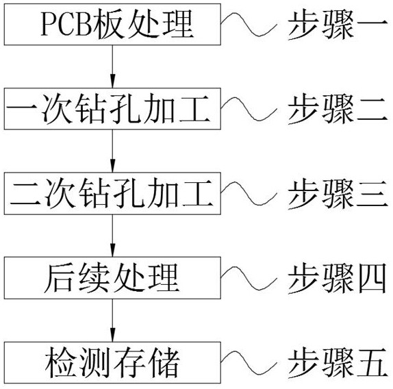
[0032] see figure 1 , the present invention provides a technical solution: a multilayer PCB board high-efficiency drilling method, including step 1, PCB board processing; step 2, primary drilling processing; step 3, secondary drilling processing; step 4, subsequent processing ; Step five, detect storage;

[0033] Wherein in the above-mentioned step one, the PCB board processing includes the following steps:

[0034] 1) Manually detect the PCB board elasticit...


PUM


Abstract

The invention discloses an efficient drilling method for a multi-layer PCB. The efficient drilling method comprises: firstly, processing the PCB; 2, conducting primary drilling machining; 3, conducting secondary drilling machining; and 4, performing subsequent treatment; 5, detecting and storing; wherein in the step 1, the elasticity, the expansion and shrinkage conditions, the air permeability and the surface lines of the PCB are manually detected, and the PCB is cleaned and dried; the copper foil liquid is poured on the PCB, the copper foil liquid is manually smeared to increase the amount of the PCB, and then the PCB is dried and stored. The efficient drilling method for the multi-layer PCB is easy to operate, the thickness of the PCB is increased through copper foil liquid, drilling machining is facilitated, positioning is conducted through a small drill bit firstly, then drilling machining is conducted through a round spiral drill bit, machining deviation is avoided, the PCB drilling speed is increased, the efficient drilling method is efficient and convenient, time and labor are saved, layered drilling is conducted, and PCB drilling deviation caused by scrap accumulation is avoided; and the scheme is provided according to different processing problems, is suitable for different production conditions and modes, and is convenient for users to process.

Description

technical field [0001] The invention relates to the technical field of PCB boards, in particular to an efficient drilling method for multilayer PCB boards. Background technique [0002] The Chinese name of PCB board is printed circuit board, also known as printed circuit board, which is an important electronic component, a support for electronic components, and a carrier for electrical connection of electronic components; It is called a printed circuit board; the traditional PCB board is directly drilled with a drill bit, and the processing is prone to deviation, which reduces the drilling speed of the PCB board, resulting in extremely inefficient drilling, and time-consuming and laborious, and debris is easy to accumulate and cause PCB board drilling. Hole deviation, and there is no solution according to different processing problems, which is inconvenient for users to process; in view of these defects, it is necessary to design an efficient drilling method for multi-layer ...

Claims


Application Information

Patent Timeline
IPC IPC(8): H05K3/00
CPCH05K3/0047
Inventor 黄春琴李炜炜
Owner 深圳市联创电路有限公司
Why Eureka
Try Eureka