
Method for protecting seed crystal layer during production of cast single crystal

A seed crystal layer and single crystal technology is applied in the field of protection of the seed crystal layer during the production of cast single crystals, which can solve the problems affecting the quality of cast single crystals, easy nucleation, etc., so as to reduce the probability of nucleation and growth, and reduce the number of nuclei. crystal, the effect of reducing the probability of dislocation

Inactive Publication Date: 2020-12-18
尹翠哲 +1
View PDF4 Cites 0 Cited by
  • Summary
  • Abstract
  • Description
  • Claims
  • Application Information

AI Technical Summary

Problems solved by technology

Due to the direct contact between the seed crystal layer and the silicon material, silicon powder and small silicon particles are easy to fall into the joints between the seed crystals, and the silicon powder and small silicon particles are easy to nucleate, and polycrystals grow between the seed crystals; Directly pressed on the seed crystal layer, the seed crystal bears a large compressive stress, resulting in the generation of dislocations, dislocations and polycrystals will seriously affect the quality of cast single crystals

Method used


Image

  • Method for protecting seed crystal layer during production of cast single crystal
  • Method for protecting seed crystal layer during production of cast single crystal
  • Method for protecting seed crystal layer during production of cast single crystal

Examples


specific Embodiment 2

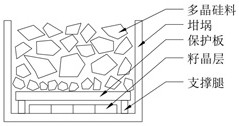
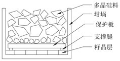
[0035] refer to figure 2 , when producing cast single crystal, provide a kind of seed crystal layer protection method, comprise the following steps:

[0036] Step a Prepare a protection plate, the size of the protection plate is 950mm×950mm×20mm, which matches the size of the G6 crucible, and the material of the protection plate is silicon material.

[0037] Step b Prepare support legs in the shape of a small cuboid, the size of the support legs is 30mm×30mm×10mm, and the material of the support legs is silicon material.

[0038] Step c: pull the single crystal ingot to remove the skin, and then cut to obtain a cuboid-shaped seed crystal. The size of the seed crystal is 158mm×158mm×20mm.

[0039] Step d: laying the seed crystal on the bottom of the crucible to form a complete seed crystal layer.

[0040] In step e, place the support legs in the shape of a small cuboid around the seed crystal layer. Only the four corners of the seed crystals are subjected to compressive stre...


PUM


Abstract

The invention discloses a method for protecting a seed crystal layer during the production of cast single crystal, which comprises the following steps of: pulling a single crystal rod straightly to remove an edge skin, cutting to obtain a cuboid seed crystal, and laying the seed crystal at the bottom of a crucible; and placing prepared supporting legs and a protection plate at the bottom of the crucible, leaving a certain gap between the seed crystal layer and the protection plate, placing a primary polycrystalline silicon material, head and tail edges and other circulating materials on the protection plate, and obtaining a cast monocrystalline silicon ingot by adopting a semi-melting process. According to the invention, silicon powder or small silicon particles can be prevented from falling into a splicing seam between seed crystals during silicon material loading, and the probability of polycrystal generation in a cast single crystal ingot can be reduced; and a certain gap is reserved between the protection plate and the seed crystal layer, and the silicon material is not directly pressed on the seed crystal layer, so that the probability of dislocation caused by pressure stresscan be reduced, and the quality of the cast monocrystalline silicon ingot is improved.

Description

technical field [0001] The invention relates to the field of photovoltaic manufacturing, in particular to a method for protecting a seed crystal layer when producing cast single crystals. Background technique [0002] At present, the general steps of producing cast single crystal are as follows: Lay a layer of single crystal seed crystal on the bottom of the crucible, install the head material, tail material, side skin and primary polysilicon material of the normal ingot on the single crystal seed crystal, and use the semi-melting process to obtain Cast single crystal. Due to the direct contact between the seed crystal layer and the silicon material, silicon powder and small silicon particles are easy to fall into the joints between the seed crystals, and the silicon powder and small silicon particles are easy to nucleate, and polycrystals grow between the seed crystals; Directly pressed on the seed crystal layer, the seed crystal bears a large compressive stress, which lea...

Claims


Application Information

Patent Timeline
IPC IPC(8): C30B29/06C30B11/00
CPCC30B11/00C30B29/06
Inventor 尹翠哲王小兵
Owner 尹翠哲
Learn More