Method for preparing multi-crystal structure lead-free interconnection welding spot by applying vibration

A technology of polycrystalline structure and solder joints, applied in metal processing equipment, manufacturing tools, welding equipment, etc., can solve the problems of large CTE mismatch, prone to failure of solder joints, and easy failure of interconnected solder joints, etc. Simple, Inexpensive Effects

Pending Publication Date: 2018-08-10
BEIJING UNIV OF TECH
View PDF2 Cites 0 Cited by
  • Summary
  • Abstract
  • Description
  • Claims
  • Application Information

AI Technical Summary

Problems solved by technology

Therefore, it will seriously affect the reliability of lead-free interconnection solder joints, and the crystal orientation of each grain in the solder joints is closely related to its reliability
For example, during the thermal cycle, if the c-axis of the β-Sn grains in the solder joint is close to parallel to the plane where the pad is located, the CTE mismatch between the solder and the pad material is large, and the interaction with this crystal or

Method used


Image

  • Method for preparing multi-crystal structure lead-free interconnection welding spot by applying vibration
  • Method for preparing multi-crystal structure lead-free interconnection welding spot by applying vibration
  • Method for preparing multi-crystal structure lead-free interconnection welding spot by applying vibration

Examples


Embodiment 1

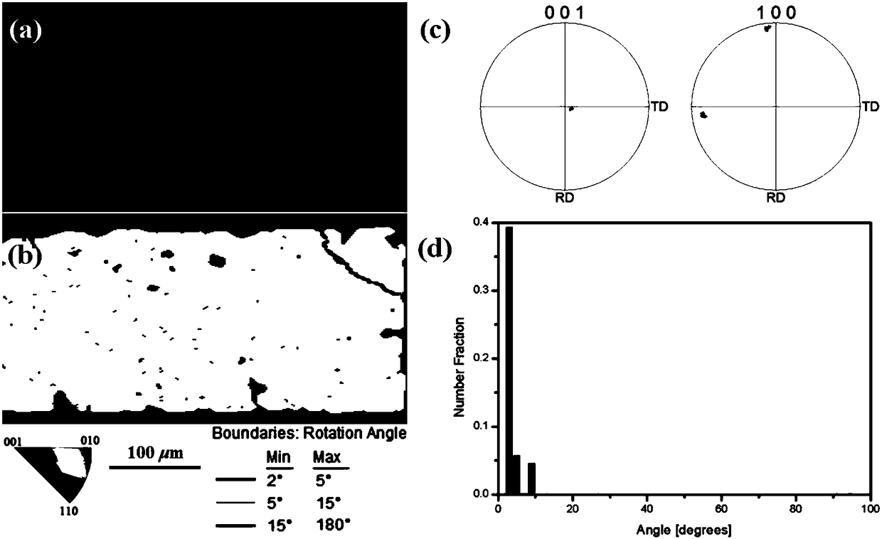
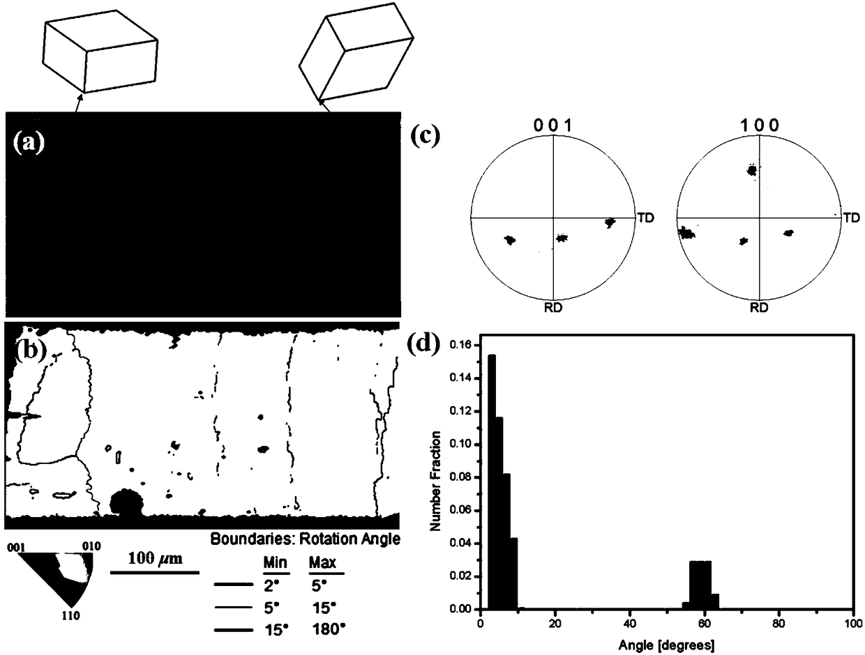
[0040] Example 1: figure 1 with 4 Explain in detail the implementation of the present invention, and combine Figure 5 , 6 , 7, 8, 9 and 10 show that the electromigration reliability of the polycrystalline solder joint structure is better than that of the single crystal solder joint.

[0041] Production of Cu / Sn3.5Ag(wt.%) / Cu linear solder joints with a cross-sectional size of 400μm×400μm and a thickness of 300μm, presenting a polycrystalline structure.

[0042] 1. The copper pad is made by wire cutting, its size is 400μm×400μm×10mm, and its purity is 99.99wt.%. Put the pad into the prepared HNO with a volume fraction of 30% 3 Soak in an aqueous solution for 30s to remove the oxide on the surface, then put the pad in an acetone solution for 60s to remove the contaminants on the surface, and then dry it for later use;

[0043] 2. Paste the double-sided adhesive on printed circuit boards (PCB), the size of the PCB is 10mm×10mm×2mm, the material is FR-4, and the copper pad to be soldered...


PUM


Abstract

The invention discloses a method for preparing a multi-crystal structure lead-free interconnection welding spot by applying vibration, and belongs to the field of material preparation and connection.The method is suitable for preparing a lead-free interconnection welding spot with polycrystalline orientations, the polycrystalline proportion of the manufactured welding spot reaches 100%, and the service reliability of the lead-free interconnection welding spot can be remarkably improved. The method has the advantage that lead-free interconnection welding spots of various structures such as a butt joint, a lap joint and a ball grid array (BGA) welding spot packaging structure can be prepared, so that the obtained lead-free interconnection welding point has the polycrystalline structure; theprocess is simple, the cost is low, except that the vibration is applied in the re-melting preparation process, the method is the same as the traditional welding spot preparation process; and meanwhile, the obtained lead-free interconnection welding spot can meet the requirements of actual application.

Description

Technical field [0001] The invention is a method for preparing polycrystalline structure lead-free interconnection solder joints by applying vibration, belongs to the field of material preparation and connection, is suitable for preparing lead-free interconnection solder joints with polycrystalline orientation, and can significantly improve lead-free interconnection solder joints The reliability of service. Background technique [0002] Solder joints play a role in mechanical connection and electrical signal transmission in microelectronic devices, and are an indispensable part of microelectronic packaging. Nowadays, on the one hand, microelectronic devices continue to develop in the direction of micro, light, thin and multifunctional; on the other hand, the packaging space has been reduced, the current density has increased, the heat generation of the chip has increased, and the working environment in which the solder joints are located has become Unprecedented harshness. More...

Claims


Application Information

Patent Timeline
IPC IPC(8): B23K1/00B23K1/19B23K1/20H01L21/607
CPCH01L24/83B23K1/0016B23K1/19B23K1/20H01L2224/83815H01L2224/83805H01L2224/83801Y02P70/50
Inventor 汉晶郭福
Owner BEIJING UNIV OF TECH
Why Eureka
Try Eureka