A method for preparing photonic crystals

A technology of photonic crystals and heating devices, applied in crystal growth, chemical instruments and methods, single crystal growth, etc., can solve the problems of low efficiency and high production cost, and achieve the effect of less process steps, low equipment requirements and high yield

Pending Publication Date: 2020-09-25
内蒙古中科启辰新材料科技有限公司
View PDF4 Cites 0 Cited by
  • Summary
  • Abstract
  • Description
  • Claims
  • Application Information

AI Technical Summary

Problems solved by technology

[0004] At present, the method of preparing photonic crystals is mainly the traditional EBL, which has high production cost and low efficiency. In addition, factors that affect the environment will also occur during the photolithography process: Wastewater: including fluorine-containing wastewater, ammonia-containing wastewater, acid Alkali wastewater, CMP wastewater; waste gas: including acid waste gas, alkaline waste gas, organic waste gas and process tail gas; solid waste and waste liquid: including waste water treatment sludge, photoresist waste liquid, organic solvent waste liquid, waste acid, etc.

Method used


Image

  • A method for preparing photonic crystals
  • A method for preparing photonic crystals

Examples


Embodiment 1

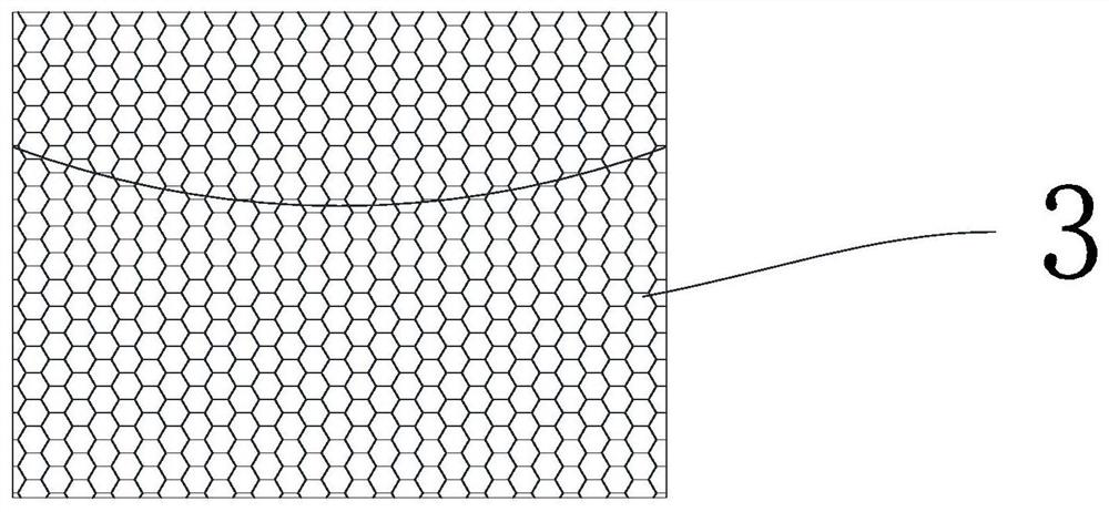
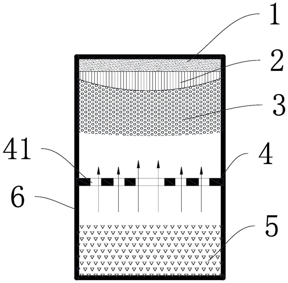
[0026] The invention provides a method for preparing photonic crystals. The preparation method comprises: in the heating device, from the bottom up, there are a pot bottom, a baffle plate with holes, a silicon carbide seed crystal and a radiator, and the heating device and the radiator are all made of graphite. production. The perforated baffle is a cylindrical perforated baffle, and at least two circles of through holes are arranged on the perforated baffle along the circumferential direction of the cylindrical baffle, and the diameter of each through hole is 6-40mm.

[0027] To heat the silicon carbide raw material placed in the bottom of the heating device, before the heating device is heated, the internal pressure is not greater than 10 Pa, and then argon gas is introduced, and after heating, the internal pressure of the heating device is maintained at 5kPa-80kPa. The heating temperature in the bottom of the heating device is 1900°C, and the heating time in the bottom of t...

Embodiment 2

[0029] The invention provides a method for preparing photonic crystals. The preparation method comprises: in the heating device, from the bottom up, there are a pot bottom, a baffle plate with holes, a silicon carbide seed crystal and a radiator, and the heating device and the radiator are all made of graphite. production. The perforated baffle is a cylindrical perforated baffle, and at least two circles of through holes are arranged on the perforated baffle along the circumferential direction of the cylindrical baffle, and the diameter of each through hole is 6-40mm.

[0030] Heat the silicon carbide raw material placed in the bottom of the heating device. Before the heating device is heated, make the internal pressure not greater than 10Pa, and then pass in argon gas. After heating, keep the internal pressure of the heating device at 50kPa. The heating temperature in the bottom of the heating device is 2000°C, and the heating time in the bottom of the pot is more than 20 hou...

Embodiment 3

[0032] The invention provides a method for preparing photonic crystals. The preparation method comprises: in the heating device, from the bottom up, there are a pot bottom, a baffle plate with holes, a silicon carbide seed crystal and a radiator, and the heating device and the radiator are all made of graphite. production. The perforated baffle is a cylindrical perforated baffle, and at least two circles of through holes are arranged on the perforated baffle along the circumferential direction of the cylindrical baffle, and the diameter of each through hole is 6-40mm.

[0033] Heat the silicon carbide raw material placed in the bottom of the heating device. Before the heating device is heated, the internal pressure is not greater than 10Pa, and then argon gas is introduced. After heating, the internal pressure of the heating device is maintained at 80kPa. The heating temperature in the bottom of the heating device is 2200°C, and the heating time in the bottom of the pot is mor...


PUM


Abstract

The invention discloses a method for preparing photonic crystals. The preparation method comprises the following steps: sequentially arranging a pot bottom, a perforated baffle, a silicon carbide seedcrystal and a radiator in a heating device from bottom to top; and heating a silicon carbide raw material placed in the pot bottom of the heating device, gasifying the silicon carbide raw material, enabling the gasified silicon carbide raw material to pass through the perforated baffle, forming liquid silicon carbide on the lower surface of the silicon carbide seed crystal, and continuously circulating to form the silicon carbide photonic crystal. The preparation method of the photonic crystal is low in equipment requirement, few in process steps, few in generated waste and simple in process,the surface of the prepared photonic crystal is free of polycrystal and impurities, and the yield is high.

Description

technical field [0001] The invention relates to the technical field of photonic crystals, in particular to a method for preparing photonic crystals. Background technique [0002] At present, optical exposure planar technology is widely used, which is one of the key technologies of integrated circuits, and is an important economic factor in the entire product manufacturing. However, the cost of applying this technology is very high, and the cost of lithography occupies the entire manufacturing process. 35% of the cost, only in terms of equipment, the establishment of an advanced integrated circuit chip processing production line needs to cost more than 1 billion US dollars. A state-of-the-art electron beam exposure machine costs millions of dollars. In addition, the processing efficiency of these technologies is relatively low, resulting in a very high cost per device. [0003] Fan et al. have theoretically calculated that photonic crystals can be used to improve the light ...

Claims


Application Information

Patent Timeline
Patent Type & Authority Applications(China)
IPC IPC(8): C30B29/36C30B23/00
CPCC30B29/36C30B23/00
Inventor 许浩郭云龙
Owner 内蒙古中科启辰新材料科技有限公司
Why Eureka
Try Eureka