Correction method of optical proximity correction model

A technology of optical proximity correction and model, which is applied in the direction of optics, originals for photomechanical processing, and photoplate making process of pattern surface, etc. It can solve the problems of distortion, deformation and deviation, and the size reduction of semiconductor devices, and achieve the improvement of precision , reduce the error, improve the effect of accuracy

Pending Publication Date: 2020-12-18
SEMICON MFG INT (SHANGHAI) CORP +1
View PDF0 Cites 0 Cited by
  • Summary
  • Abstract
  • Description
  • Claims
  • Application Information

AI Technical Summary

Problems solved by technology

[0004] However, with the rapid development of integrated circuit design, the size of semiconductor devices continues to shrink, and distortion will occur during the transfer of graphics to the wafer. deformation and deviation

Method used


Image

  • Correction method of optical proximity correction model
  • Correction method of optical proximity correction model
  • Correction method of optical proximity correction model

Examples


Embodiment Construction

[0035] It is known from the background art that optical proximity correction is used to form expected target patterns on a wafer. However, the accuracy of optical proximity correction still needs to be improved.

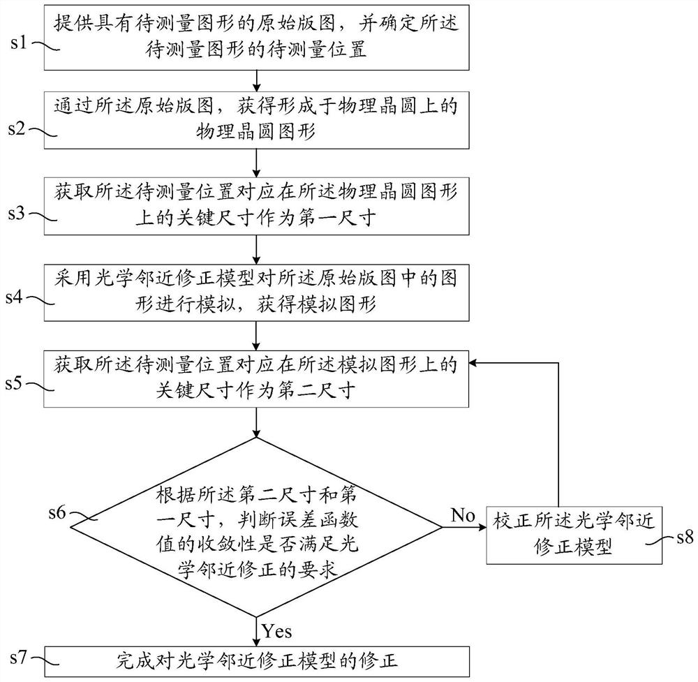
[0036] refer to figure 1 , shows a schematic flowchart of an optical proximity correction model calibration method.

[0037] The steps of the optical proximity correction model calibration method include:

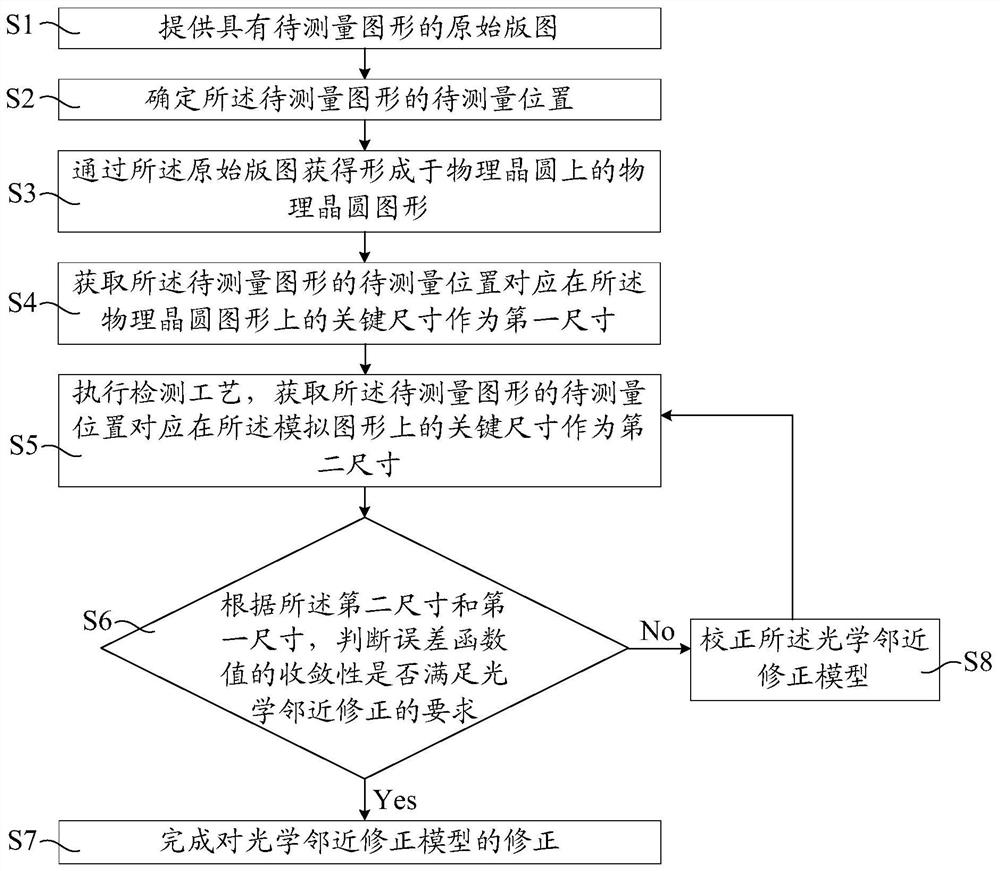
[0038] Execute step s1, provide the original layout (layout) with the pattern to be measured, and determine the position to be measured of the pattern to be measured;

[0039] Execute step s2, obtain the physical wafer pattern formed on the physical wafer through the original layout;

[0040] Executing step s3, acquiring the critical dimension (CD) corresponding to the location to be measured on the physical wafer pattern as a first dimension;

[0041]Execute step s4, using the optical proximity correction model to simulate the graphics in the original layout ...


PUM


Abstract

The invention discloses a correction method of an optical proximity correction model. The correction method comprises the following steps: providing an original layout with a to-be-measured graph; determining a to-be-measured position of the to-be-measured graph; obtaining a physical wafer pattern formed on the physical wafer through the original layout; obtaining a key size, corresponding to theto-be-measured position, on the physical wafer graph as a first size; executing a detection process: simulating the original layout by adopting an OPC model to obtain a simulated graph; selecting a first to-be-measured area on the simulation graph according to the to-be-measured position, and collecting measurement data of a plurality of key sizes in the first to-be-measured area; according to themeasurement data of the plurality of key sizes and a first size type, obtaining a key size, corresponding to the to-be-measured position, on the simulation graph as a second size; judging whether convergence of an error function value meets a requirement of optical proximity correction or not according to the second size and the first size; and when the requirement is not met, correcting an OPC model, and returning to the step of executing the detection process. According to the invention, OPC precision is improved.

Description

technical field [0001] Embodiments of the present invention relate to the field of semiconductor manufacturing, and in particular, to a method for correcting an optical proximity correction model. Background technique [0002] In the integrated circuit manufacturing process, photolithography technology is the driving force for the development of integrated circuit manufacturing process, and it is also one of the most complex technologies. Compared with other individual manufacturing technologies, the improvement of lithography technology is of great significance to the development of integrated circuits, and the process accuracy of lithography technology directly affects the yield rate of semiconductor products. [0003] Before the photolithography process starts, the wafer layout will be copied onto the mask plate by specific equipment, and then the light of a specific wavelength (such as 248 nm ultraviolet light) will be generated by the photolithography equipment to conve...

Claims


Application Information

Patent Timeline
IPC IPC(8): G03F1/36
CPCG03F1/36
Inventor 杜杳隽
Owner SEMICON MFG INT (SHANGHAI) CORP
Why Eureka
Try Eureka