Micro-led array based on micropatterned graphene, its preparation method, and display device

A micro-pattern, graphene technology, applied in semiconductor devices, electrical components, circuits, etc., to achieve the effects of strong operability, stress relief, and simple process

Active Publication Date: 2022-05-27
CHANGCHUN INST OF OPTICS FINE MECHANICS & PHYSICS CHINESE ACAD OF SCI
View PDF0 Cites 0 Cited by
  • Summary
  • Abstract
  • Description
  • Claims
  • Application Information

AI Technical Summary

Problems solved by technology

[0005] In view of this, the present invention proposes a Micro-LED array based on micropatterned graphene, its preparation method, and a display device to solve the defects existing in the existing Micro-LED light-emitting devices

Method used


Image

  • Micro-led array based on micropatterned graphene, its preparation method, and display device
  • Micro-led array based on micropatterned graphene, its preparation method, and display device
  • Micro-led array based on micropatterned graphene, its preparation method, and display device

Examples


Embodiment Construction

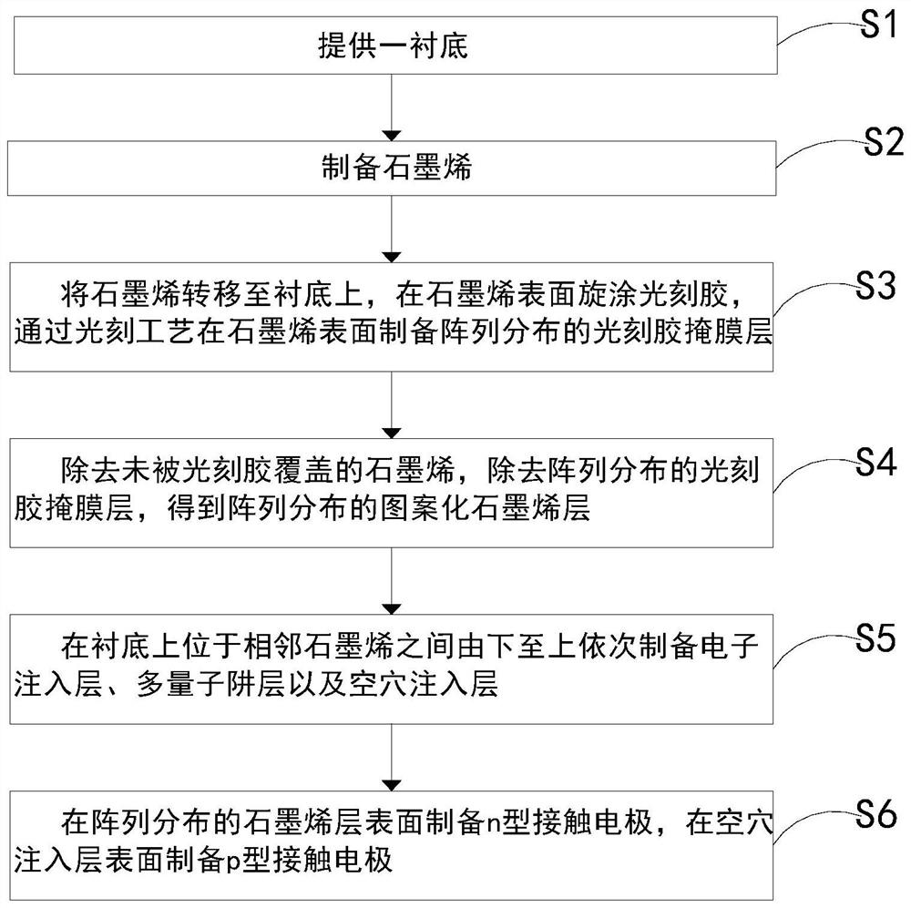
[0039] The technical solutions in the embodiments of the present invention will be clearly and completely described below in conjunction with the embodiments of the present invention. Obviously, the described embodiments are only a part of the embodiments of the present invention, but not all of the embodiments. Based on the embodiments of the present invention, all other embodiments obtained by persons of ordinary skill in the art without creative efforts shall fall within the protection scope of the present invention.

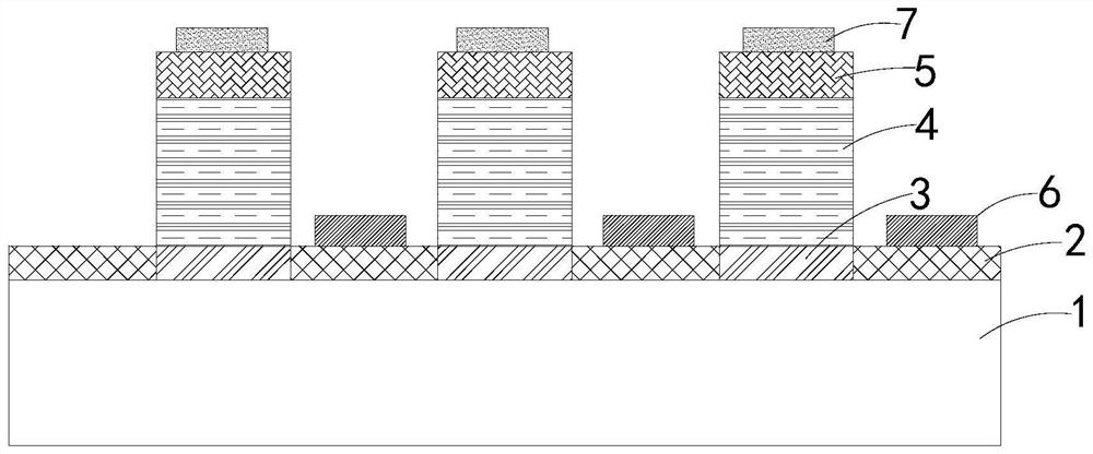
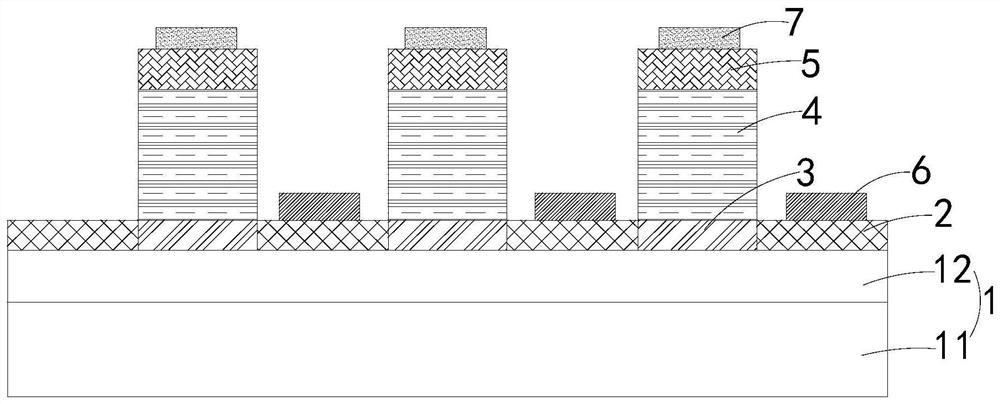
[0040] like figure 1 As shown, the present invention provides a Micro-LED array based on micropatterned graphene, comprising:

[0041] substrate 1;

[0042] The patterned graphene layer 2, the array of which is distributed on one side of the substrate 1;

[0043] The electron injection layer 3 is located on the side of the substrate 1 close to the patterned graphene layer 2, and the electron injection layer 3 is projected on the substrate 1 between the adja...


PUM

PropertyMeasurementUnit
thicknessaaaaaaaaaa
thicknessaaaaaaaaaa
thicknessaaaaaaaaaa

Abstract

The invention provides a Micro-LED array based on micro-patterned graphene, a preparation method thereof, and a display device. The array includes: a substrate; a patterned graphene layer, the array of which is distributed on one side of the substrate; an electron injection layer located at The substrate is close to the side of the patterned graphene layer, and the electron injection layer is projected on the substrate between adjacent patterned graphene layers; the multi-quantum well layer is located on the side of the electron injection layer away from the substrate; the hole injection layer, The n-type contact electrode is located on the side of the patterned graphene layer away from the substrate; the p-type contact electrode is located on the side of the hole injection layer away from the substrate. In the Micro-LED array of the present invention, the good conductivity of graphene can also be directly used as the bottom electrode of the Micro-LED, and the contact between the patterned graphene layer and the electron injection layer forms a good conductive path, so that electrons can pass through the patterned graphene layer. Efficient injection into Micro‑LEDs.

Description

technical field [0001] The invention relates to the technical field of preparation of LEDs, in particular to a Micro-LED array based on micro-patterned graphene, a preparation method thereof, and a display device. Background technique [0002] Group III nitride materials mainly include InN, GaN and AlN, which can be mixed in any proportion to form ternary and quaternary alloys, and their direct band gaps are adjustable at 0.7-6.2 eV. Based on this, group III nitride materials as the light-emitting layer of LEDs can realize broadband light emission from deep ultraviolet to visible red light, and the corresponding Micro-LED can meet the application requirements of full-color display. Compared with the more mature OLEDs technical solutions on the market, they have the advantages of high luminous brightness, low energy consumption and long service life, and have high application potential in TV, smart phones, car navigation, AR / VR and other fields. [0003] At present, the main...

Claims


Application Information

Patent Timeline
Patent Type & Authority Patents(China)
IPC IPC(8): H01L27/15H01L33/00H01L33/42
CPCH01L27/156H01L33/42H01L33/007H01L2933/0016
Inventor 黎大兵陈洋孙晓娟蒋科张山丽贾玉萍
Owner CHANGCHUN INST OF OPTICS FINE MECHANICS & PHYSICS CHINESE ACAD OF SCI
Why Eureka
Try Eureka