Supercharge Your Innovation With Domain-Expert AI Agents!

Systems and methods for performing dynamic on-chip calibration of memory control signals

A memory system, memory array technology, applied in the field of system-on-a-chip with improved calibration, can solve problems such as threats to multi-level cell capabilities, verification failures, failures, etc.

Pending Publication Date: 2020-12-22
MICRON TECH INC
View PDF1 Cites 0 Cited by
  • Summary
  • Abstract
  • Description
  • Claims
  • Application Information

AI Technical Summary

Problems solved by technology

As can be seen, this early reservation threatens multilevel cell capability and tight V T distribution, and may result in a significant shift 262 of the distribution, such that a verification failure occurs, e.g., at 270
Potentially, read operations after a given time since the programming event could also fail due to this effect if no calibration mechanism is provided

Method used


Image

  • Systems and methods for performing dynamic on-chip calibration of memory control signals
  • Systems and methods for performing dynamic on-chip calibration of memory control signals
  • Systems and methods for performing dynamic on-chip calibration of memory control signals

Examples


Embodiment Construction

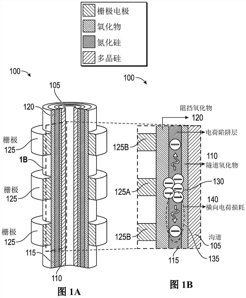
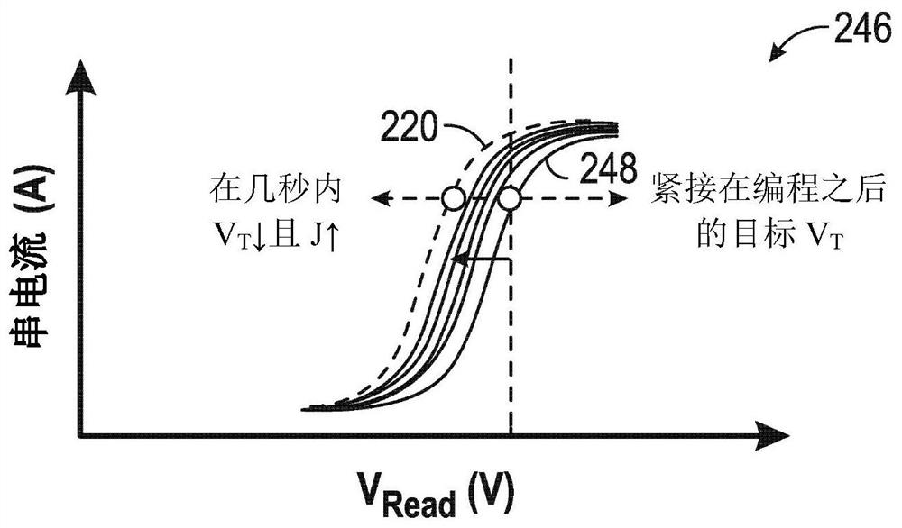
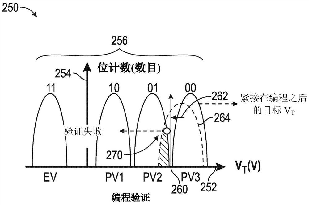
[0023] The following disclosure describes various embodiments of systems and methods of dynamically calibrating memory (read) control signals, eg, during increases in word line voltage. According to one embodiment, an exemplary method may include using an internal node, such as a wordline regulator output or return feedback line or a replica of the wordline, as a proxy for the local wordline voltage. In one or more other embodiments, the proxy signal may be converted to digital code and determined in the background even before it is needed for calibration. In accordance with the disclosed techniques, calibration of read control signals such as pass voltages and word line read verify voltages can be performed during the increase in the word line voltage without impact or loss in read / program time. Thus, systems and methods consistent with the disclosed techniques can avoid performance loss while enabling even NAND memory cells that exhibit the effects of rapid charge depletion ...


PUM


Abstract

The application relates to systems and methods for performing dynamic on-chip calibration of memory control signals. Systems and methods of dynamically calibrating memory control signals during increase of wordline voltage for memory technologies subject to charge loss are disclosed. In one aspect, an exemplary method may comprise using an internal node, such as a wordline regulator output or return feedback line or a replica of the wordline, as proxy for the local wordline voltage. In one or more further embodiments, the proxy signal may be converted to digital signal or code and even determined in the background before the signal is needed for calibration. As a function of the disclosed technology, calibration of memory control signals, such as pass voltage and wordline read-verify voltage, may be performed during increase of the wordlines voltage with no impact or penalty on read / program time.

Description

technical field [0001] The present disclosure relates generally to multi-level flash memory control, and more particularly to on-chip systems and methods for performing improved calibration of memory control signals. Background technique [0002] Various modern semiconductor memories, such as three-dimensional NAND flash memory, may suffer from early retention in the lateral direction (ie, rapid exponential charge depletion over time from a programming event) due to shared charge trapping layers. Figures 1A to 1B is a diagram illustrating a three-dimensional NAND flash memory known in the art. Such as Figure 1A As shown in , a three-dimensional NAND flash memory structure 100 may include (extending from the core) a polysilicon channel layer 105, a tunnel oxide layer 110 surrounding the polysilicon layer 105, a charge trapping layer associated with the tunnel oxide layer 110 layer 115 , such as an O / N / O stacked silicon nitride layer, a blocking oxide layer 120 surrounding ...

Claims


Application Information

Patent Timeline
Patent Type & Authority Applications(China)
IPC IPC(8): G11C8/08G11C16/08G11C16/04
CPCG11C8/08G11C16/08G11C16/0483G11C16/26G11C16/30G11C16/32G11C16/3418G11C16/3459G11C5/145G11C29/021G11C29/028G11C2029/1202G11C11/5621G11C2207/2254G11C11/4085G11C11/4074
Inventor M·皮卡尔迪
Owner MICRON TECH INC
Features
  • R&D
  • Intellectual Property
  • Life Sciences
  • Materials
  • Tech Scout
  • Unparalleled Data Quality
  • Higher Quality Content
  • 60% Fewer Hallucinations
Learn More