Manufacturing method of packaging structure

A technology of packaging structure and manufacturing method, which is applied in semiconductor/solid-state device manufacturing, electrical components, circuits, etc., can solve the problems of the overall quality of the packaging structure, difficulty in manually placing circuit boards, and high production costs, and achieve excellent thermal stability. The effect of uniform force and low cost

Active Publication Date: 2020-12-22
ANHUI LONGXINWEI TECH CO LTD
View PDF17 Cites 1 Cited by
  • Summary
  • Abstract
  • Description
  • Claims
  • Application Information

AI Technical Summary

Problems solved by technology

[0002] After the chip is processed, due to the small size and thinness of the chip, it will be easily scratched and damaged if no external protection is applied. Moreover, because the size of the chip is small, it is not easy to manually place it on the circuit board; The circuit pins of the circuit are connected to the external joints with wires so as to be connected with other devices; the packaged product is called a package structure; the production method of the package structure in the prior art

Method used


Image

  • Manufacturing method of packaging structure
  • Manufacturing method of packaging structure
  • Manufacturing method of packaging structure

Examples


Embodiment Construction

[0040] The technical solutions of the present invention will be clearly and completely described below in conjunction with the embodiments. Apparently, the described embodiments are only some of the embodiments of the present invention, not all of them. Based on the embodiments of the present invention, all other embodiments obtained by persons of ordinary skill in the art without creative efforts fall within the protection scope of the present invention.

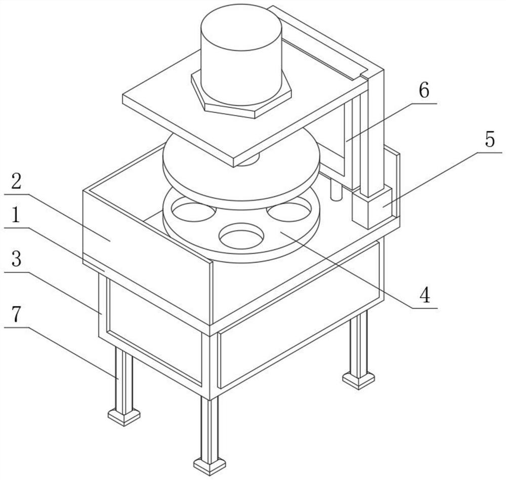
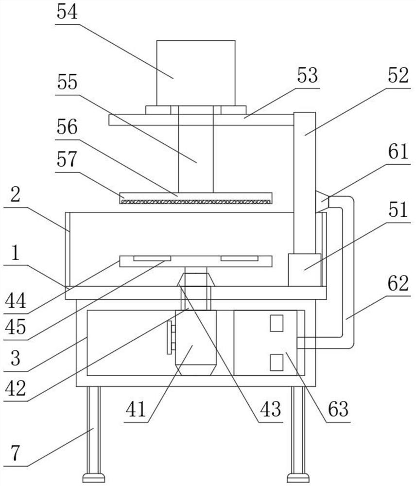
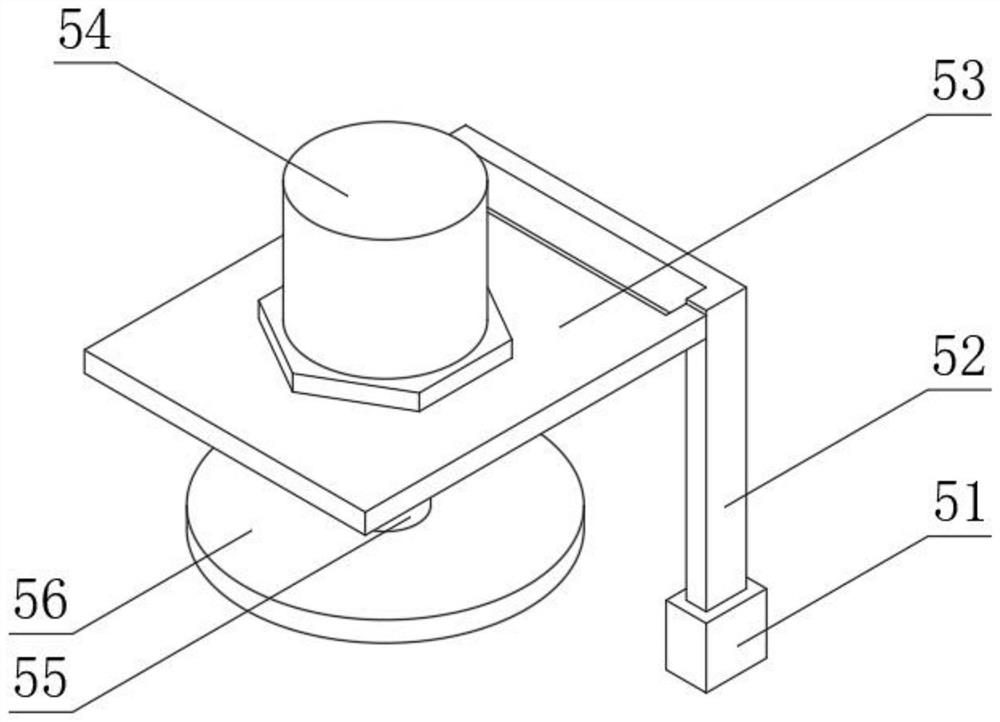
[0041] Such as Figure 1-3 As shown, a manufacturing method of a packaging structure includes the following steps:

[0042] Step S1: Grind the back of the wafer coming out of the wafer factory through wafer grinding equipment to reduce the thickness of the wafer to the thickness required for packaging; when grinding the wafer, it is necessary to stick tape on the front of the wafer to protect the circuit area and grind the back of the wafer at the same time ;After grinding, remove the tape and measure the thickness of the ...


PUM


Abstract

The invention discloses a manufacturing method of a packaging structure, and the method comprises the following steps: S1, carrying out the back grinding of a wafer from a wafer factory through wafergrinding equipment, so as to reduce the thickness of the wafer to a thickness required by packaging; pasting an adhesive tape on the front surface of the wafer to protect a circuit area and grinding the back surface at the same time during wafer grinding; after grinding, removing the adhesive tape, and measuring the thickness of the wafer; pasting the thinned chip on a thin film with a metal ring,and sending the thin film to a scribing machine for scribing; S2, after scribing is completed, mounting and pasting the wafer on the blue film, so the wafer does not scatter even if the wafer is cutoff; and cutting the whole wafer into independent chips one by one through wafer cutting. The method is low in cost, and the economic benefit can be greatly improved; meanwhile, in the packaging process, the silicon wafer polishing effect is good, and dust pollution can be effectively reduced; moreover, the packaging structure is processed, so that the overall quality of the packaging structure can be greatly improved.

Description

technical field [0001] The invention relates to the technical field of chip packaging, in particular to a method for manufacturing a packaging structure. Background technique [0002] After the chip is processed, due to the small size and thinness of the chip, it will be easily scratched and damaged if no external protection is applied. Moreover, because the size of the chip is small, it is not easy to manually place it on the circuit board; The circuit pins of the circuit are connected to the external joints with wires so as to be connected with other devices; the packaged product is called a package structure; the production method of the package structure in the prior art, in the process of processing, the production cost is relatively high, As a result, the economic benefit is low; moreover, there are flaws such as burrs on the surface of the packaged structure, which can easily affect the overall quality of the packaged structure; at the same time, a large amount of dus...

Claims


Application Information

Patent Timeline
IPC IPC(8): H01L21/56H01L21/304H01L21/02
CPCH01L21/56H01L21/304H01L21/02096H01L21/67126
Inventor 黄晓波
Owner ANHUI LONGXINWEI TECH CO LTD
Why Eureka
Try Eureka