FPGA on-chip clock duty ratio test method and clock self-test FPGA

A test method and technology of duty cycle, applied in the field of integrated circuits, can solve problems such as limiting the maximum measurement frequency, increasing test cost, and limited I/O interface performance, achieving the effect of reducing test cost and reducing index requirements

Pending Publication Date: 2020-12-22
CHENGDU SINO MICROELECTRONICS TECH CO LTD
View PDF0 Cites 0 Cited by
  • Summary
  • Abstract
  • Description
  • Claims
  • Application Information

AI Technical Summary

Problems solved by technology

However, testing under high-precision conditions requires the use of an oscilloscope with a very high sampling rate, which increases the cost of testing
At the same time, limited by the performance of the I / O interface, the maximum measurement frequency that can be achieved is limited
The IBIS interface characteristics of the I / O interface will also affect the duty cycle test results

Method used


Image

  • FPGA on-chip clock duty ratio test method and clock self-test FPGA
  • FPGA on-chip clock duty ratio test method and clock self-test FPGA
  • FPGA on-chip clock duty ratio test method and clock self-test FPGA

Examples


Embodiment 1

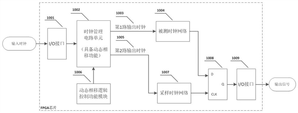
[0070] see Figure 8 , in this example figure 1 On the basis of a typical test system architecture, an output logic detection function circuit can be added without using an oscilloscope.

[0071] Because the maximum operating frequency that the logic circuit resources in the FPGA chip can achieve is far lower than the upper frequency limit that the clock management circuit unit can achieve. Therefore, the operating clock frequency of the output logic detection function circuit (8009) cannot be too high, and combined with engineering application experience, it can usually be set to an operating frequency of 200MHz or below. In order to meet this requirement, the operating frequency of the second output clock (8005) can be reduced, so that the frequency of the first output clock and the second output clock can maintain an integer multiple relationship, and the operating frequency of the second output clock can be lower than Outputting the operating clock frequency of the logi...

Embodiment 2

[0074] This embodiment describes the phase shift control process in detail, see Figure 9 ~ Figure 17 .

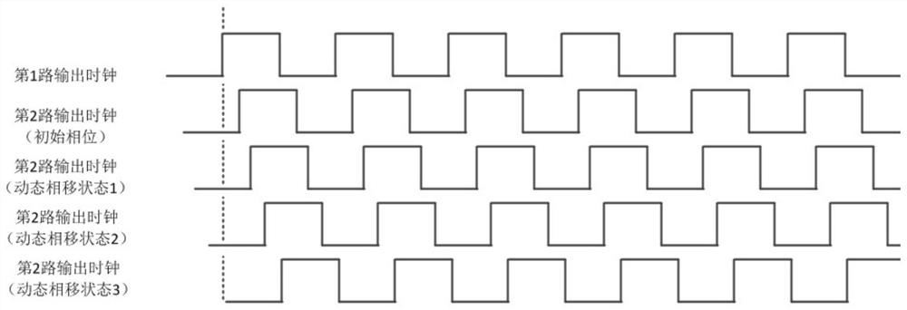
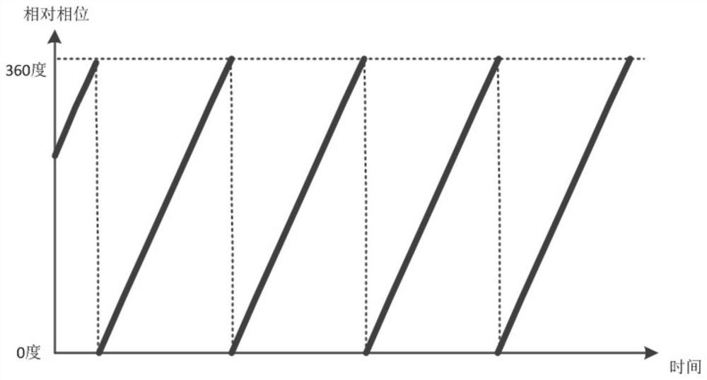
[0075] Figure 9 As shown, in the whole process of the duty cycle test, set Ps as a fixed phase adjustment step value, keep the CLK clock signal of the flip-flop for K clock cycles (K is an integer) in each phase state, and trigger The device samples the D input signal and outputs the Q signal.

[0076] Figure 10 ~ Figure 16 The principle of phase change between the CLK terminal input and the Q terminal output of the D flip-flop is shown in a step-by-step manner. The present invention scans the duty cycle of the high-frequency clock signal in the chip through low-speed phase scanning, greatly reduces the test cost, and can guarantee the test accuracy up to tens of picoseconds at the same time.


PUM


Abstract

The invention discloses an FPGA on-chip clock duty ratio test method and a clock self-test FPGA, and relates to the integrated circuit technology. The clock self-test FPGA comprises an I/O interface unit, a clock management circuit unit and a tested clock network, and is characterized by further comprising a D trigger, the input end of the clock management circuit unit is connected with a clock source, and the first output end of the clock management circuit unit is connected with the input end of the tested clock network; the output end of the tested clock network is connected to the D end ofthe D trigger, the second output end of the clock management circuit unit is connected with the input end of the sampling clock network, the output end of the sampling clock network is connected to the CLK end of the D trigger, the output end of the D trigger is connected to an output logic detection function circuit, the output logic detection function circuit is connected with the I/O interfaceunit, and a dynamic phase shift logic function control module is connected with the clock management circuit unit. According to the invention, the index requirements on test instruments and equipmentare reduced.

Description

technical field [0001] The present invention relates to integrated circuit technology. Background technique [0002] Through the FPGA I / O test interface, using pulse pattern generators, signal sources and other equipment to input clock signals to the device under test, and then using an oscilloscope to measure the duty cycle parameters of the output clock signal is the most conventional test method. By comparing the input clock signal and the output clock signal, the parameter performance change of the duty cycle of the clock signal can be measured. The test method is easy to operate and record. However, testing under high-precision conditions requires the use of an oscilloscope with a very high sampling rate, which increases the cost of testing. At the same time, limited by the performance of the I / O interface, the maximum measurement frequency that can be achieved is limited. The IBIS interface characteristics of the I / O interface will also have an impact on the duty cy...

Claims


Application Information

Patent Timeline
Patent Type & Authority Applications(China)
IPC IPC(8): H03K5/19
CPCH03K5/19
Inventor 贾楫丛伟林何相龙孙海蔡莹卓
Owner CHENGDU SINO MICROELECTRONICS TECH CO LTD
Why Eureka
Try Eureka