Wafer failure analysis method

A failure analysis and wafer technology, applied in electronic circuit testing, measuring devices, instruments, etc., can solve the problems of increasing time cost, difficulty in sample preparation, and affecting the efficiency of sample preparation.

Active Publication Date: 2021-01-05
YANGTZE MEMORY TECH CO LTD
View PDF6 Cites 2 Cited by
  • Summary
  • Abstract
  • Description
  • Claims
  • Application Information

AI Technical Summary

Problems solved by technology

[0003] In related technologies, in order to avoid damage to the metal layer, manual polishing is often used to polish the silicon in the sample. However, manual polishing will increase the time cost and the difficulty of sample preparation, thereby affecting the efficiency of sample preparation.

Method used


Image

  • Wafer failure analysis method
  • Wafer failure analysis method
  • Wafer failure analysis method

Examples


Embodiment Construction

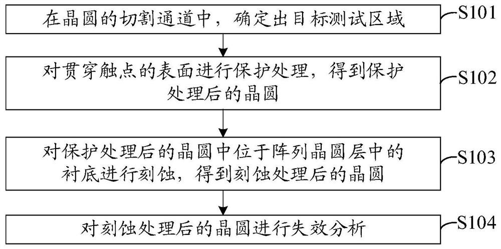
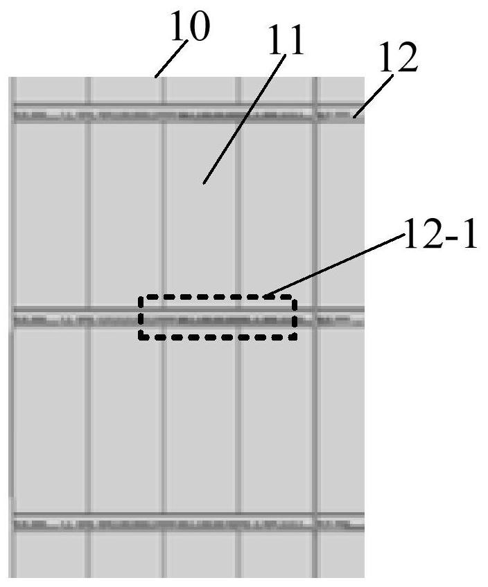
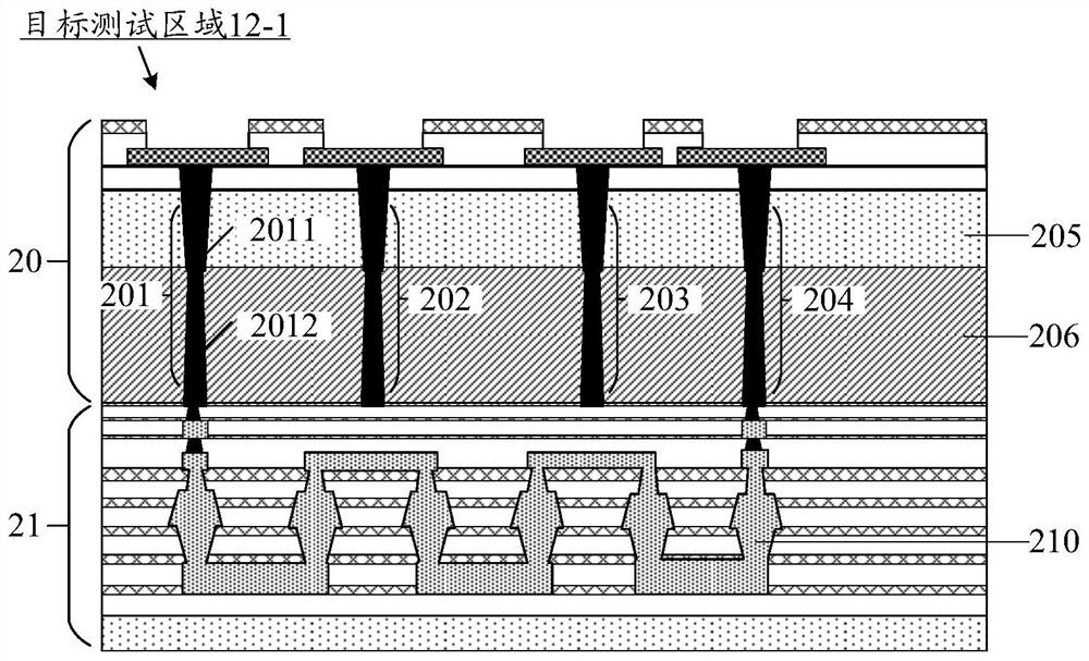
[0054] In order to make the purpose, technical solutions and advantages of the embodiments of the present application clearer, the specific technical solutions of the invention will be further described in detail below in conjunction with the drawings in the embodiments of the present application. The following examples are used to illustrate the present application, but not to limit the scope of the present application.

[0055]As indicated in this application and claims, the terms "a", "an", "an" and / or "the" do not refer to the singular and may include the plural unless the context clearly indicates an exception. Generally speaking, the terms "comprising" and "comprising" only suggest the inclusion of clearly identified steps and elements, and these steps and elements do not constitute an exclusive list, and the method or device may also contain other steps or elements.

[0056] Spatial terms such as "on...", "below...", "underneath", "below...", "on...", "above", etc., can...


PUM


Abstract

The embodiment of the invention discloses a wafer failure analysis method, which comprises the steps of determining a target test area in a cutting channel of a wafer, the wafer comprising a driving wafer layer and an array wafer layer which are stacked, wherein the array wafer layer comprises a stacking layer located on the driving wafer layer and a substrate located on the side, deviating from the driving wafer layer, of the stacking layer, and the target test area comprises a through contact penetrating through the array wafer layer and a test structure formed in the driving wafer layer andlocated below the through contact; performing protection processing on the surface of the through contact to obtain a wafer after protection processing; etching the substrate, located in the array wafer layer, in the wafer after the protection processing to obtain a wafer after the etching processing; and performing failure analysis on the wafer after the etching processing.

Description

technical field [0001] The embodiment of the present application relates to the field of semiconductor technology, and relates to but not limited to a wafer failure analysis method. Background technique [0002] For the test area (Test Key, TSK) of the three-dimensional flash memory structure, in the physical failure analysis (Physical Failure Analysis, PFA), it is necessary to use the Inductively Coupled Plasma (ICP) technology to remove the silicon in the sample for sample preparation . When the etching time of the ICP exceeds 10 minutes, the metal layer located under the Through Array Contact & Through Silicon Contact (TAC & TSC) will be damaged. [0003] In the related art, in order to avoid damage to the metal layer, manual polishing is often used to polish the silicon in the sample. However, manual polishing will increase the time cost and the difficulty of sample preparation, thereby affecting the efficiency of sample preparation. Contents of the invention [0004...

Claims


Application Information

Patent Timeline
Patent Type & Authority Applications(China)
IPC IPC(8): G01R31/28
CPCG01R31/2851G01R31/2898
Inventor 王君易
Owner YANGTZE MEMORY TECH CO LTD
Why Eureka
Try Eureka