Terahertz radio frequency signal detector based on metasurface optical antenna and preparation method
An optical antenna and radio frequency signal technology, applied in the field of signal detection, can solve the problems of large volume, slow response, narrow detection band, etc., achieve good detection performance, reduce cost, and increase the effect of contact area
- Summary
- Abstract
- Description
- Claims
- Application Information
AI Technical Summary
Problems solved by technology
Method used
Image
Examples
Embodiment 1
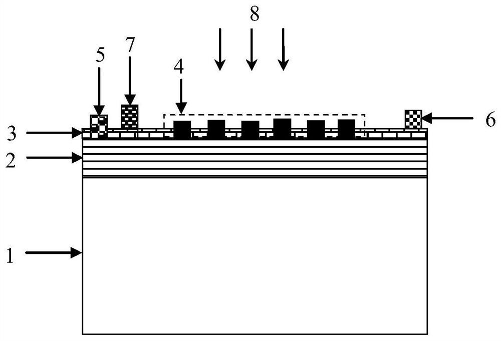
[0032] refer to figure 1 , a terahertz radio frequency signal detector based on a metasurface optical antenna, comprising: a substrate layer 1, a doped layer 2, a silicon dioxide layer 3, a metasurface optical antenna layer 4, an ohmic electrode 5, and a Schottky electrode 6 and common electrodes7. Wherein, the doped layer 2 is formed on the substrate layer 1, the silicon dioxide layer 3 is made on the doped layer 2, the metasurface optical antenna layer 4 is made on the doped layer 2, and the ohmic electrode 5 is made on the doped layer. On the layer 2, the Schottky electrode 6 is made on the silicon dioxide layer 3, the common electrode 7 is made on the silicon dioxide layer 3, and the ohmic electrode 5 and the Schottky electrode 6 are respectively located on the surface of the metasurface optical antenna layer 4. At the left and right ends, the common electrode 7 and the Schottky electrode 6 are respectively located at the left and right ends of the metasurface optical ant...
Embodiment 2
[0041] A method for preparing a terahertz radio frequency signal detector based on a metasurface optical antenna proposed in Embodiment 1, comprising the following steps:
[0042] S1. Si ions are implanted on the substrate 1 by metal-organic compound chemical vapor deposition method, and the doping concentration is 1×10 16 cm -3 ~9×10 18 cm -3 , thereby forming a doped layer 2 with a thickness of 1 μm to 2 μm; in this embodiment, the substrate layer 1 is semi-insulating gallium arsenide, and the doped layer 2 is N-type gallium arsenide as an example;
[0043] S2, preparing a silicon dioxide layer 3 on the doped layer 2 by a plasma-enhanced chemical vapor deposition method, the thickness of which is 100nm-300nm;
[0044] S3. Photoetching the ohmic electrode contact hole pattern on the silicon dioxide layer 3 through a positive resist process, and using a wet etching process to etch the silicon dioxide layer at the position of the ohmic electrode contact hole pattern, and the...
Embodiment 3
[0055] refer to Figure 10 , this embodiment provides another terahertz radio frequency signal detector based on a metasurface optical antenna, including: a substrate layer, a first doped layer, a first silicon dioxide layer, a first metasurface optical antenna layer, a first Ohmic electrode, first Schottky electrode, first common electrode, second doped layer, second silicon dioxide layer, second metasurface optical antenna layer, second ohmic electrode, second Schottky electrode, second Common electrodes; wherein the first doped layer is located on the substrate layer, the first silicon dioxide layer, the first metasurface optical antenna layer, and the first ohmic electrode are located on the first doped layer, The first Schottky electrode and the first common electrode are located on the first silicon dioxide layer; the first Schottky electrode and the first common electrode are all connected to the first metasurface optical antenna layer connected, the first metasurface ...
PUM
| Property | Measurement | Unit |
|---|---|---|
| width | aaaaa | aaaaa |
| thickness | aaaaa | aaaaa |
| thickness | aaaaa | aaaaa |
Abstract
Description
Claims
Application Information


