Laminating device for semiconductor preparation

A semiconductor and layer-using technology, which is applied in the field of lamination devices for semiconductor preparation, can solve problems such as low work efficiency and slow lamination speed, and achieve the effects of improving work efficiency, prolonging service life, and ensuring stability

Inactive Publication Date: 2021-01-15
广州夕千科技有限公司
View PDF0 Cites 0 Cited by
  • Summary
  • Abstract
  • Description
  • Claims
  • Application Information

AI Technical Summary

Problems solved by technology

[0002] Semiconductors refer to materials whose conductivity is between conductors and insulators at room temperature. Semiconductors are used in integrated circuits, consumer electronics, communication systems, photovoltaic power generation, lighting, high-power power conversion and other fields. For example, diodes are devices made of semiconductors. , no matter from the perspective of technology or economic development, the importance of semiconductors is very huge. The core units of most electronic products, such as computers, mobile phones or digital recorders, are closely related to semiconductors. , common semiconductor materials include silicon, germanium, gallium arsenide, etc., silicon is the most influential one in the application of various semiconductor materials, and a lamination device is required in semiconductor preparation; lamination refers to whether to use or not Adhesive, a method of combining two or more layers of the same or different materials into a whole by heating and pressure, also known as lamination molding, refers to combining multiple layers of the same or different materials under heat and pressure An overall molding processing method; however, the lamination device in the prior art has a simple structure and can only laminate a single semiconductor material, the lamination speed is slow, and the work efficiency is low

Method used


Image

  • Laminating device for semiconductor preparation
  • Laminating device for semiconductor preparation
  • Laminating device for semiconductor preparation

Examples


Embodiment Construction

[0056] The following will clearly and completely describe the technical solutions in the embodiments of the present invention with reference to the accompanying drawings in the embodiments of the present invention. Obviously, the described embodiments are only some, not all, embodiments of the present invention. Based on the embodiments of the present invention, all other embodiments obtained by persons of ordinary skill in the art without making creative efforts belong to the protection scope of the present invention.

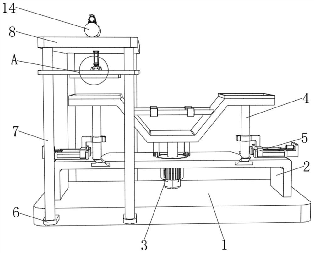
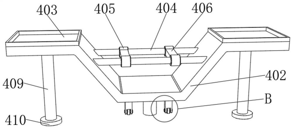
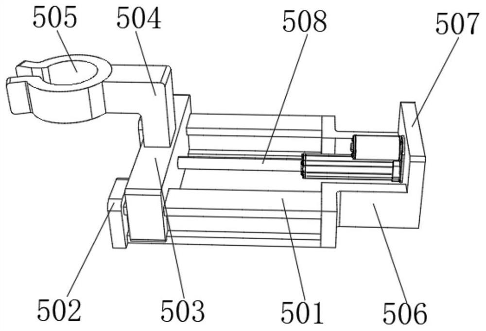
[0057] see Figure 1-5 , the present invention provides a technical solution: a lamination device for semiconductor preparation, including a base plate 1, a U-shaped support plate 2 is fixedly connected to the middle of the upper surface of the base plate 1, and a drive motor is arranged in the middle of the lower surface of the U-shaped support plate 2 3. The model of the drive motor 3 is Y112M-2, the middle part of the upper surface of the U-shaped support p...


PUM


Abstract

The invention relates to the technical field of semiconductor preparation, and discloses a laminating device for semiconductor preparation. The device comprises a bottom plate, a U-shaped supporting plate is fixedly connected to the middle of the upper surface of the bottom plate, a driving motor is arranged in the middle of the lower surface of the U-shaped supporting plate, and an adjustable discharging device is arranged in the middle of the upper surface of the U-shaped supporting plate. Sliding type fixing devices are arranged on the left side and the right side of the upper surface of the U-shaped supporting plate correspondingly, mounting feet are fixedly connected to the left sides of the front face and the back face of the bottom plate correspondingly, and guide columns are fixedly connected to the middles of the upper surfaces of the mounting feet. According to the laminating device for semiconductor preparation, the driving motor drives a rotating shaft to rotate, so that the rotating shaft drives a supporting bracket to rotate, the supporting bracket rotates to exchange the positions of two sets of storage frames, uninterrupted processing of two sets of semiconductor materials is achieved, the processing speed of the semiconductor materials is increased, the working efficiency is improved, and the practicability of the laminating device is improved.

Description

technical field [0001] The invention relates to the technical field of semiconductor preparation, in particular to a laminating device for semiconductor preparation. Background technique [0002] Semiconductors refer to materials whose conductivity is between conductors and insulators at room temperature. Semiconductors are used in integrated circuits, consumer electronics, communication systems, photovoltaic power generation, lighting, high-power power conversion and other fields. For example, diodes are devices made of semiconductors. , no matter from the perspective of technology or economic development, the importance of semiconductors is very huge. The core units of most electronic products, such as computers, mobile phones or digital recorders, are closely related to semiconductors. , common semiconductor materials include silicon, germanium, gallium arsenide, etc., silicon is the most influential one in the application of various semiconductor materials, and a laminat...

Claims


Application Information

Patent Timeline
IPC IPC(8): B32B37/06B32B37/10H01L21/67
CPCB32B37/06B32B37/10H01L21/67011
Inventor 蒋双娣
Owner 广州夕千科技有限公司
Why Eureka
Try Eureka