Low-power system and method of Internet of Things chip

An Internet of Things chip and low power consumption technology, which is applied in power management, energy consumption reduction, machine-to-machine/machine-type communication services, etc., can solve the problem of low power consumption of chips, so as to promote wide application and reduce overall Effects of power consumption and extended battery life

Active Publication Date: 2021-01-15
上海赛昉科技有限公司
View PDF6 Cites 2 Cited by
  • Summary
  • Abstract
  • Description
  • Claims
  • Application Information

AI Technical Summary

Problems solved by technology

[0004] Aiming at the deficiencies of the prior art, the present invention discloses a low-power consumption system and method for an Internet of Things chip, which solves the problem of a traditional Internet of Things chip that needs fast response. The problem that the power consumption of the chip cannot be reduced enough in the scene

Method used


Image

  • Low-power system and method of Internet of Things chip
  • Low-power system and method of Internet of Things chip
  • Low-power system and method of Internet of Things chip

Examples


Embodiment 1

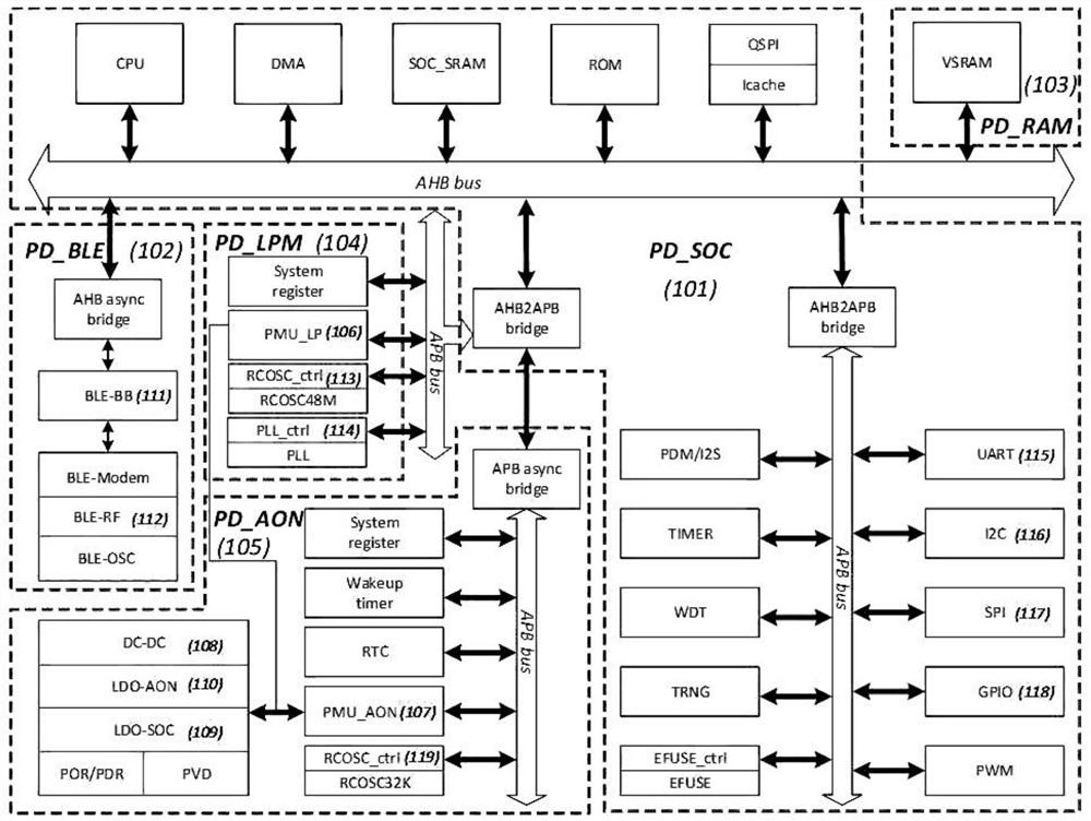
[0030] This embodiment discloses a low power consumption architecture of an IoT chip, see figure 1 As shown, the IoT chip designed with this architecture includes five power supplies including PD_SOC power domain (101), PD_BLE power domain (102), PD_RAM ​​power domain (103), PD_LPM power domain (104) and PD_AON power domain (105). domain composition. The description of the five power domains is as follows:

[0031] PD_SOC power domain (101): the components of the system on chip including CPU, memory, bus, DMA and peripherals, which are the parts that realize the main functions of the system on chip;

[0032] PD_BLE power domain (102): Bluetooth low energy components including BLE baseband, modem, RF and clock generator, which is a part to realize Bluetooth low energy communication function;

[0033] PD_RAM ​​power domain (103): includes a group of components including SRAM with retention and powerdown modes, which can realize the combination of various low-power modes such a...

Embodiment 2

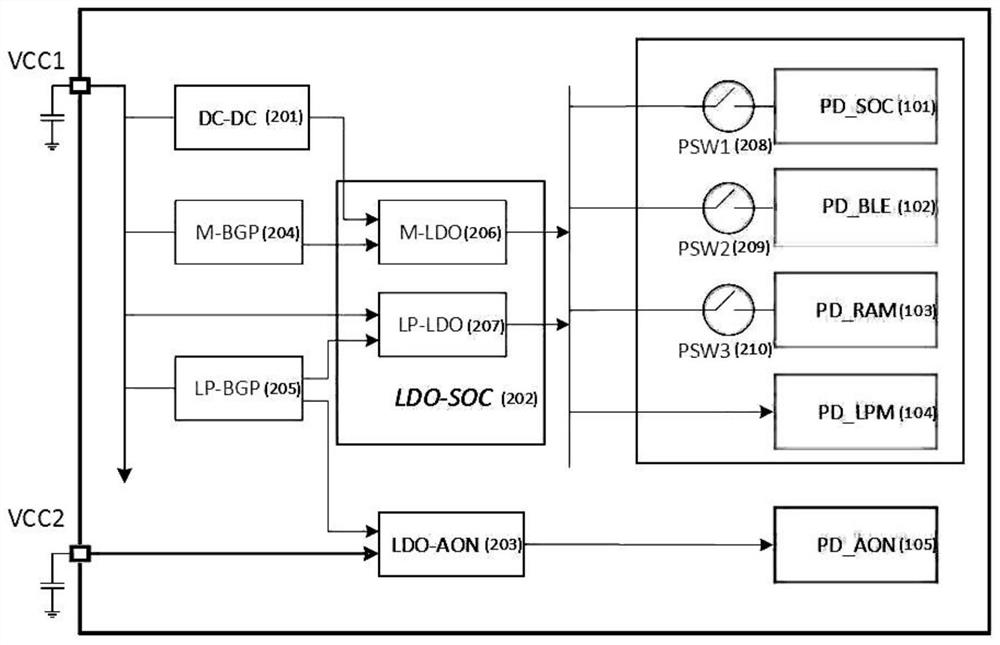
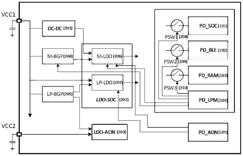
[0037] This embodiment discloses a low power consumption architecture of an Internet of Things chip. According to the above power domain division, different power domains have their own dedicated power supply sources. See figure 2 and image 3 As shown, the components of the power supply network include two external power supply pins VCC1 and VCC2, DC-DC (201), LDO-SOC (202), LDO-AON (203), MBGP (204), LPBGP (205), PSW1 (208), PSW2 (209) and PSW3 (210).

[0038] Among them, the voltages of the two external power supply pins VCC1 and VCC2 are VCC1: 3V and VCC2: 1.2V;

[0039] Wherein, the DC-DC (201) steps down the voltage of VCC1 from 3V to 1.5V, and provides it to the MLDO (206) in the LDO-SOC (202);

[0040]Among them, LDO-SOC (202) is a dual power supply component composed of two LDOs, MLDO (206) is a power supply for normal operation, and MBGP (204) provides a reference voltage. LPLDO (207) is the power supply source used for the low power consumption state, and the re...

Embodiment 3

[0046] This embodiment discloses a low power consumption architecture of an Internet of Things chip. There are 7 power consumption modes in total. The working conditions of each power supply in different power consumption modes are shown in the following table:

[0047]

[0048] The low-power architecture of an IoT chip disclosed in this embodiment has 7 power consumption modes in total, and the working conditions of each power domain in different power consumption modes are shown in the following table:

[0049]

[0050] Among the 7 power consumptions, we will focus on the Hibernate mode. Based on the design of dual power supply switching, the Hibernate mode is a unique mode for implementing a low-power architecture of an IoT chip that takes into account both response speed and power consumption. The Hibernate mode is divided into two modes: Hibernate_1 and Hibernate_2.

[0051] The working principle of Hibernate_1 schema is described below. All power domains are power...


PUM


Abstract

The invention relates to the technical field of Internet of Things chips, in particular to a low-power system and method for an Internet of Things chip, and the system comprises a PD_SOC power domainfor achieving the main functions of a system on chip; a PD_BLE power supply domain for realizing a low-power Bluetooth communication function; a PD_RAM power supply domain for realizing overall poweron and down and formed by combining a plurality of low-power modes such as retention, powerdown and the like; a PD_LPM power supply domain for realizing global configuration, global clock reset and power consumption management; and a PD_AON power supply domain for realizing global configuration, low-frequency clock and global reset, awakening and power supply/power consumption management of the always on domain. By using a double-power switching scheme and utilizing the low-power characteristic of the low-power power supply and the characteristics of relatively high response speed, precision and power supply capability of the main power supply, under mutual combination, the Internet of Things chip realizes two goals of low power consumption and quick response in a low-power mode needing quick response, so that the reliability of the Internet of Things chip is improved. The requirement of people for prolonging the endurance time of electronic products is met, and wider application of the electronic products is promoted.

Description

technical field [0001] The invention relates to the technical field of Internet of Things chips, in particular to a low power consumption system and method for Internet of Things chips. Background technique [0002] In the low-power consumption mode that requires fast response, the traditional single power supply method does not take the power consumption of the power supply itself as the research object. It is difficult to balance the two factors. [0003] In the low power consumption mode of the IoT chip, there is a contradiction between the low power consumption level and the response speed. In the low power consumption mode that requires fast response, this solution can significantly reduce power consumption. Contents of the invention [0004] Aiming at the deficiencies of the prior art, the present invention discloses a low power consumption system and method for an Internet of Things chip, which solves the problem that the traditional Internet of Things chip cannot ...

Claims


Application Information

Patent Timeline
Patent Type & Authority Applications(China)
IPC IPC(8): H04W52/02H04W4/70H04W4/80
CPCH04W52/0261H04W4/70H04W4/80Y02D30/70
Inventor 佘磊
Owner 上海赛昉科技有限公司
Why Eureka
Try Eureka