Flip Mini/Micro-LED chip easy to weld and preparation method and packaging method of flip Mini/Micro-LED chip

A packaging method and chip technology, applied in the direction of electrical components, circuits, semiconductor devices, etc., can solve the problems of poor final products, high precision of solder paste brushing method, easy overflow, etc., to avoid excessive or too small dosage, shorten Effect of preventing solder overflow between packages

Pending Publication Date: 2021-01-19
FOSHAN NATIONSTAR SEMICON
View PDF0 Cites 1 Cited by
  • Summary
  • Abstract
  • Description
  • Claims
  • Application Information

AI Technical Summary

Problems solved by technology

The current welding problems include: 1. Chip displacement: the chip moves after soldering, and it is necessary to reduce the movement of the bare chip after soldering; 2. Chip rotation: because the distance between the Mini / Micro-LED chip itself is only 0.8mm, 0.6mm, 0.4mm Even smaller, then during the soldering process, the chip itself is easy to rotate in the atmosphere environment, which has a bad effect; 3. High void rate: At present, after nitrogen reflow soldering, solder paste with low void rate is used, and the void rate after soldering is also controlled to About 10%; for ordinary solder paste, the void rate may reach more than 15% after soldering. If the void rate is too high, long-term use may cause defective products due to thermal conductivity or reliability problems
There are more than 9,000 chips on a circuit board. It is a big thing that there are several defects that lead to the defect of the final product.
[0004] In addition, the existing methods of applying solder and flux are generally divided into dot solder paste method and brush solder paste method. Among them, the solder paste dot method is fast, low in accuracy, uses a large amount of glue, is easy to overflow, and the chip is easy to shift and short circuit; brushing solder paste method has high accuracy, but the speed is slow and the price of the machine is high
Therefore, the solder paste step for Mini / Micro-LED chips has great barriers to the promotion of Mini / Micro-LED chip flip-chip products

Method used


Image

  • Flip Mini/Micro-LED chip easy to weld and preparation method and packaging method of flip Mini/Micro-LED chip

Examples


Embodiment Construction

[0038] In order to make the object, technical solution and advantages of the present invention clearer, the present invention will be further described in detail below in conjunction with the accompanying drawings.

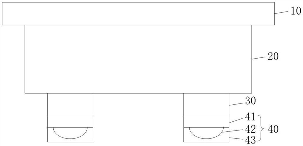
[0039] see figure 1 ,本发明提供的一种易于焊接的倒装Mini / Micro-LED芯片,包括衬底10、设于衬底10上的发光结构20、设于发光结构20上的电极30、以及设于电极30上的焊接层40,其中,所述倒装Mini / Micro-LED芯片的尺寸小于100μm。

[0040] 所述焊接层40包括焊料层41、设于焊料层41上的助焊层42、以及设于焊料层41和助焊层42上并将助焊层42包裹的保护层43。

[0041] 本发明的焊料层用于结合电极和基板,因此所述焊料层的材料必须为导电材料;此外,为了提高电极与基板之间的结合力,所述焊料层还用于填补电极与基板之间的空隙,减少芯片与基板之间的不平整,减少芯片与基板之间的空洞率和增加焊接层的可靠度,因此所述焊料层的材料必须具有一定的软度。优选的,所述焊料层的材料选自锡铅焊料、银焊料、铜焊料和纯锡焊料中的一种或几种。

[0042] 其中,焊料层的厚度对于芯片的后续焊接、封装起着重要的作用,若焊料层的厚度过厚,则焊接时容易溢出、导致芯片漏电;若焊料层的厚度过小,则芯片与基板结合不牢固,降低焊接良率。

[0043] 优选的,所述焊料层的厚度为10~100μm。更优的,所述焊料层的厚度为20~80μm。最优的,所述焊料层的厚度为40~60μm。

[0044] 具体的,本发明采用黄光蒸镀或钢网印刷的方式在电极上形成焊料层。在LED的晶圆阶段,本发明同时在多个发光结构的在电极上形成焊料层,与逐个LED芯片点锡膏与刷锡膏的封装方法相比,效率大大提高,且可以通过控制焊料层的厚度,精准控制锡膏的用量,避免锡膏用量过多或过小,有效保证芯片与基板的结合力,同时防止芯片旋转移位,从而提高LED芯片与基板的焊接良率。

[0045]The existing wel...


PUM

PropertyMeasurementUnit
thicknessaaaaaaaaaa
thicknessaaaaaaaaaa
thicknessaaaaaaaaaa

Abstract

The invention discloses an easy-to-weld flip Mini / Micro-LED chip and a preparation method and a packaging method thereof. The chip comprises a substrate, a light-emitting structure arranged on the substrate, an electrode arranged on the light-emitting structure, and a welding layer arranged on the electrode. The Mini / Micro-LED chip disclosed by the invention is easy to weld and package, high in packaging efficiency, high in yield and low in cost.

Description

technical field [0001] 本发明涉及发光二极管技术领域,尤其涉及一种易于焊接的倒装Mini / Micro-LED芯片及其制备方法、封装方法。 Background technique [0002] 倒装LED芯片具有免封装的特点,因此大大降低了下游封装厂的打线焊接时间和成本。虽然可以省略打线焊接的步骤,但还是需要涂抹焊料和助焊剂在电极上,以将LED芯片的电极与基板形成导电连接。 [0003] Mini / Micro-LED芯片的焊盘更小、锡膏量更少、芯片更小,对焊接设备的要求、温度均匀度等工艺参数提出了更高的要求。目前焊接出现的问题包括:1、芯片位移:芯片焊接之后有移动,需要减少裸芯片焊接后的移动;2、芯片旋转:因为Mini / Micro-LED芯片本身间距只有0.8mm、0.6mm、0.4mm甚至更小,那么在焊接过程中,芯片本身在气氛环境下容易旋转,影响不良;3、空洞率高:目前氮气回流焊焊接之后,采用低空洞率锡膏,焊接后空洞率也就控制到10%左右;普通的锡膏,焊接后空洞率可能达到15%以上,空洞率太高,长期使用因为导热效果或可靠性问题可能会导致产品不良。一块电路板上面有9000多颗芯片,有几个不良导致最终产品的不良是很大的一件事。 [0004] 此外,现有焊料和助焊剂的涂附方式一般分为点锡膏法和刷锡膏法,其中,点锡膏法速度快,精准度低,用胶量多,容易溢出,芯片容易移位和短路;刷锡膏法精准度高,但速度慢,且机台价格高。因此,Mini / Micro-LED芯片的刷锡膏步骤对于推行Mini / Micro-LED芯片倒装产品有极大的壁垒。 Contents of the invention [0005] 本发明所要解决的技术问题在于,提供一种易于焊接的倒装Mini / Micro-LED芯片及其制备方法,易于焊接封装,封装效率高、良率高、成本低。 [0006] 本发明还要解决的技术问题在于,提供一种易于焊接的倒装Mini / Micro-LED芯片的封装方法,封装效率高、良率高、成本低。 [0007] 为了解决上述技术问题,本发明提供了一种易于焊接的倒装Mini / Micro-LED芯片,包括衬底、设于衬底上的发光结构、设于发光结构上的电极、以及设于电极上的焊接层; [0008] 所述焊接层包括焊料层、设于焊料...

Claims


Application Information

Patent Timeline
Patent Type & Authority Applications(China)
IPC IPC(8): H01L33/62
CPCH01L33/62H01L2933/0066
Inventor 崔永进仇美懿
Owner FOSHAN NATIONSTAR SEMICON
Why Eureka
Try Eureka