Equipment capable of carrying out index test on photoelectric products and semiconductor elements

A technology for index testing and optoelectronic products, which is applied in the direction of single semiconductor device testing, non-contact testing, and components of electrical measuring instruments, etc. Natural environment, resource reduction, cost reduction effects

Inactive Publication Date: 2021-01-22
宁波锦锐能源科技有限公司
View PDF0 Cites 0 Cited by
  • Summary
  • Abstract
  • Description
  • Claims
  • Application Information

AI Technical Summary

Problems solved by technology

[0004] The current optoelectronic products and semiconductor components have fewer functions for index testing equipment, and it is not convenient to use, and the cost of using test equipment will be relatively high, which will lead to a significant increase in consumption
[0005] Existing equipment that can test the indicators of optoelectronic products and semiconductor components does not have the ability to recycle

Method used


Image

  • Equipment capable of carrying out index test on photoelectric products and semiconductor elements
  • Equipment capable of carrying out index test on photoelectric products and semiconductor elements
  • Equipment capable of carrying out index test on photoelectric products and semiconductor elements

Examples


Embodiment Construction

[0033] The following will clearly and completely describe the technical solutions in the embodiments of the present invention with reference to the accompanying drawings in the embodiments of the present invention. Obviously, the described embodiments are only some, not all, embodiments of the present invention. Based on the embodiments of the present invention, all other embodiments obtained by persons of ordinary skill in the art without making creative efforts belong to the protection scope of the present invention.

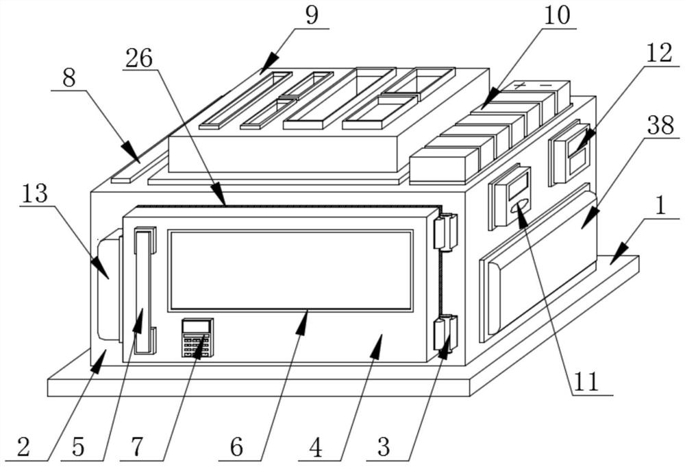
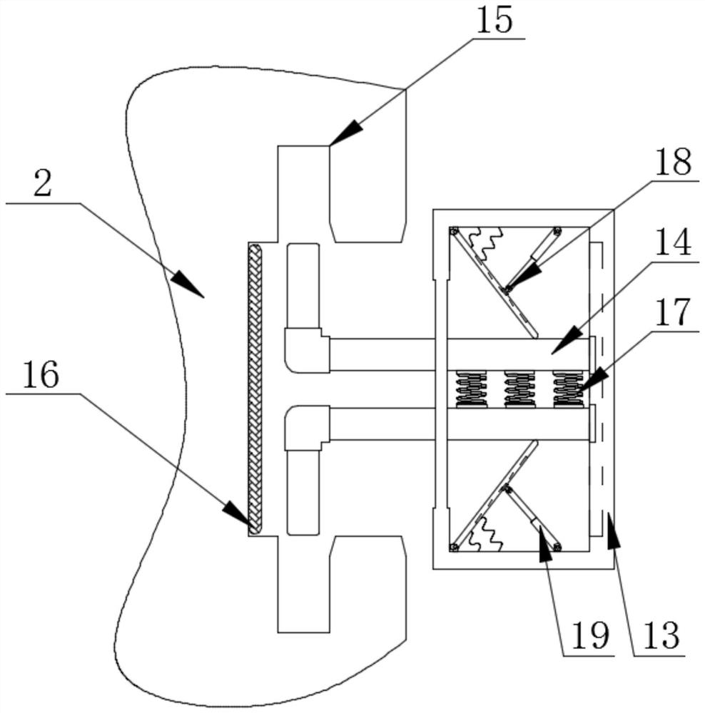
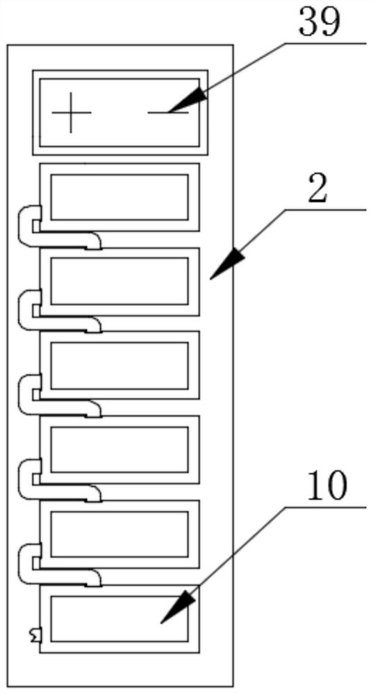
[0034] see Figure 1-8 , the embodiment of the present invention provides a technical solution: a device for index testing of optoelectronic products and semiconductor components, including a base plate 1 and a detection box 2, the middle part of the top of the base plate 1 is fixedly connected with the bottom of the detection box 2, and the detection box 2 One side of the front surface is fixedly connected with a hinge 3, and the surface of the detection box ...


PUM


Abstract

The invention discloses equipment capable of performing index test on photoelectric products and semiconductor elements. The equipment comprises a bottom plate and a detection box, wherein the middleportion of the top of the bottom plate is fixedly connected with the bottom of the detection box, one side of the front surface of the detection box is fixedly connected with a hinge, the bottom of the left side of the front surface of a box door is fixedly connected with a password input device, and the middle portion of the top of the detection box is fixedly connected with a semiconductor slot.The invention relates to the technical field of electronic product testing. According to the equipment capable of performing index testing on the photoelectric product and the semiconductor element,the index testing equipment can have a resource recovery capability, so that the cost is lower when the index testing equipment is used for testing, consumed resources are correspondingly reduced so as to achieve the effects of reducing the cost and protecting the natural environment, the whole work becomes more environment-friendly and the cost is low, a worker can use the index testing equipmentmore easily, and people can use the index testing equipment conveniently.

Description

technical field [0001] The invention relates to the technical field of electronic product testing, in particular to a device capable of performing index testing on optoelectronic products and semiconductor components. Background technique [0002] Semiconductors refer to materials whose conductivity is between conductors and insulators at room temperature. Semiconductors are used in integrated circuits, consumer electronics, communication systems, photovoltaic power generation, lighting, high-power power conversion and other fields. For example, diodes are devices made of semiconductors. , no matter from the perspective of technology or economic development, the importance of semiconductors is very huge. The core units of most electronic products, such as computers, mobile phones or digital recorders, are closely related to semiconductors. , common semiconductor materials include silicon, germanium, gallium arsenide, etc. Silicon is the most influential one in the applicatio...

Claims


Application Information

Patent Timeline
IPC IPC(8): G01R31/265G01R1/04
CPCG01R1/0408G01R31/2601
Inventor 王姜愉
Owner 宁波锦锐能源科技有限公司
Why Eureka
Try Eureka