
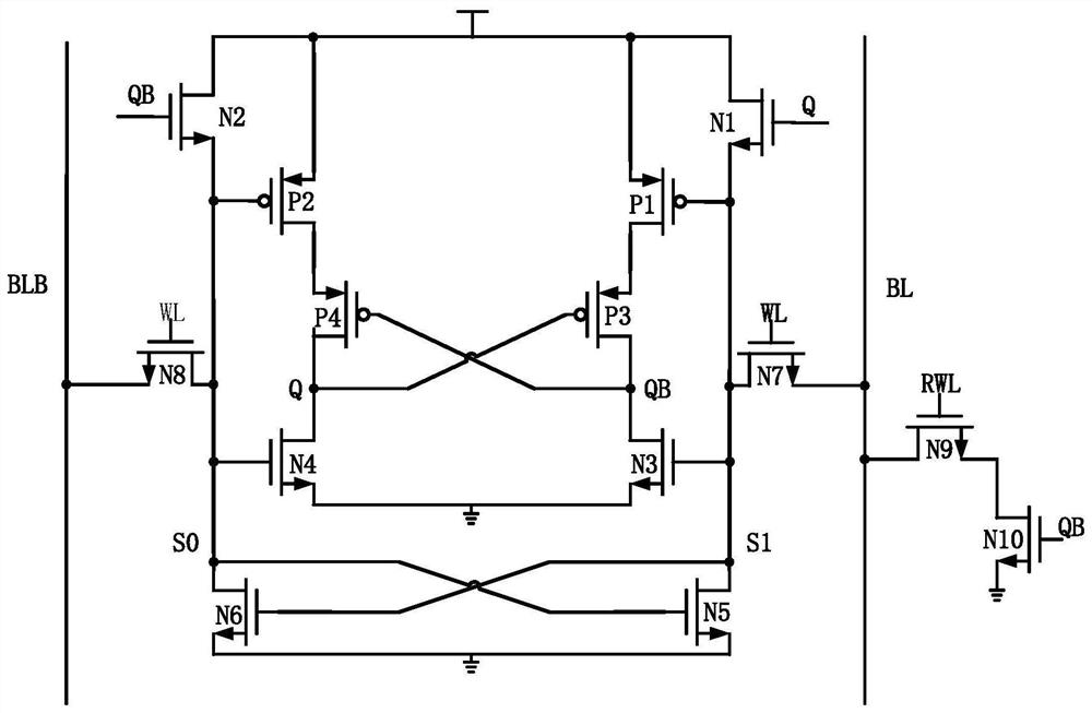
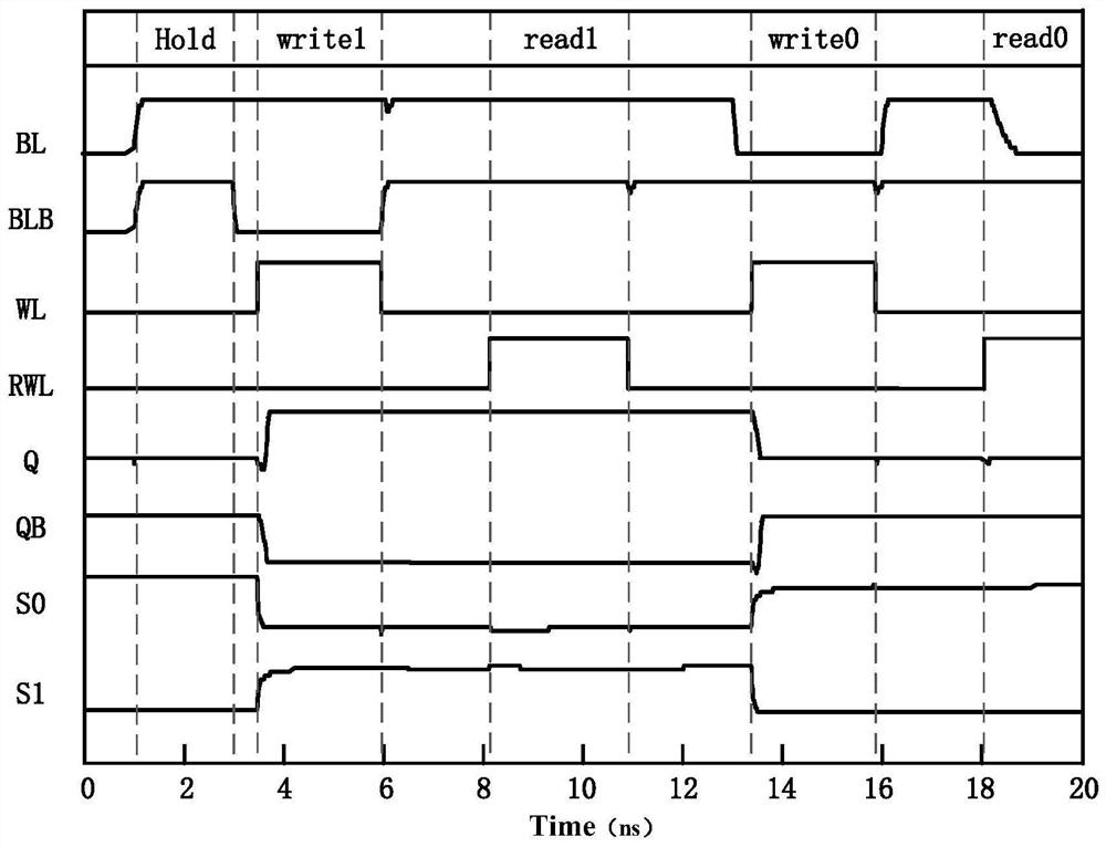
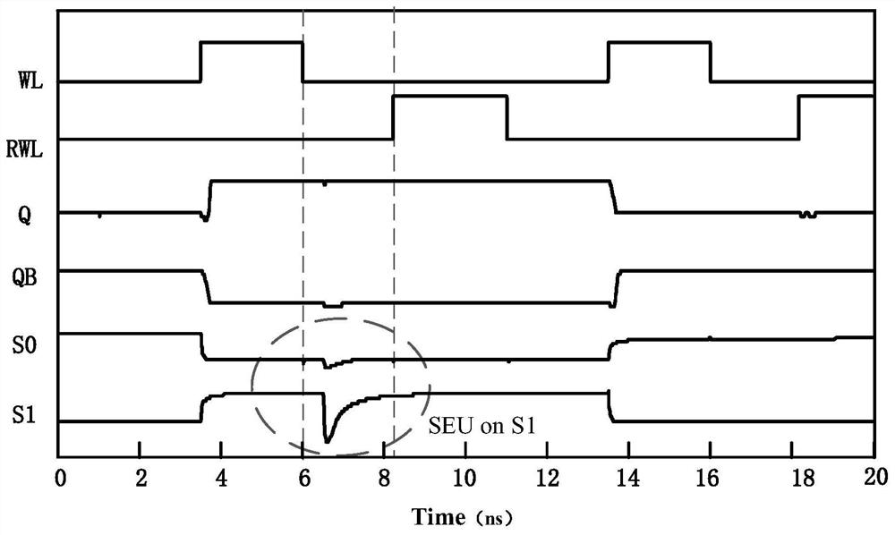
Read-write separated 14T radiation-resistant SRAM (Static Random Access Memory) storage unit circuit structure

A memory cell circuit, read-write separation technology, applied in information storage, static memory, digital memory information and other directions, can solve the problems of large area of ​​SRAM array module, soft errors, high packaging density, etc. The ability to resist multi-particle flipping, improve the ability to read and write, and optimize the effect of cell stability

Active Publication Date: 2021-01-22
ANHUI UNIVERSITY
View PDF6 Cites 1 Cited by
  • Summary
  • Abstract
  • Description
  • Claims
  • Application Information

AI Technical Summary

Problems solved by technology

[0003]Static Random Access Memory (Static Random Access Memory, abbreviated as SRAM), due to the high sensitivity per bit, the node capacitance is low, and the SRAM array module is in the chip It occupies the largest area, has a high packing density and lacks an error shielding mechanism, so it has the highest probability of soft errors due to single event effects in the space environment, and there is no effective solution in the prior art

Method used


Image

  • Read-write separated 14T radiation-resistant SRAM (Static Random Access Memory) storage unit circuit structure
  • Read-write separated 14T radiation-resistant SRAM (Static Random Access Memory) storage unit circuit structure
  • Read-write separated 14T radiation-resistant SRAM (Static Random Access Memory) storage unit circuit structure

Examples


Embodiment Construction

[0022] The technical solutions in the embodiments of the present invention will be clearly and completely described below in conjunction with the accompanying drawings in the embodiments of the present invention. Obviously, the described embodiments are only some of the embodiments of the present invention, not all of them. Based on the embodiments of the present invention, all other embodiments obtained by persons of ordinary skill in the art without making creative efforts belong to the protection scope of the present invention.

[0023] Embodiments of the present invention will be further described in detail below in conjunction with the accompanying drawings, as figure 1 Shown is a schematic structural diagram of a 14T anti-radiation SRAM storage unit circuit with read-write separation provided by an embodiment of the present invention. The circuit includes ten NMOS transistors and four PMOS transistors. PMOS transistors are recorded as P1~P4 in turn, where:

[0024] PMOS...


PUM


Abstract

The invention discloses a read-write separated 14T radiation-resistant SRAM (Static Random Access Memory) storage unit circuit structure which comprises ten NMOS (N-channel Metal Oxide Semiconductor)transistors and four PMOS (P-channel Metal Oxide Semiconductor) transistors which are sequentially marked as N1 to N10 and P1 to P4, the PMOS transistors P1 and P2 are used as pull-up tubes, peripheral storage nodes are controlled by S1 and S0, and the PMOS transistors P3 and P4 are crossly coupled; NMOS transistors N3 and N4 are used as pull-down tubes, and peripheral nodes are cross-coupled by NMOS transistors N5 and N6; NMOS transistors N1 and N2 serve as pull-up tubes, peripheral storage nodes S0 and S1 reinforce internal nodes Q and QB by controlling NMOS transistors N3 and N4, peripheralnodes are all surrounded by the NMOS transistors, and the structure is called as a polarity reinforcing structure. The circuit structure can effectively optimize the stability of the unit, improve the read-write capability of the unit, and improve the single-particle and multi-particle upset resistance of the storage unit.

Description

technical field [0001] The invention relates to the technical field of integrated circuit design, in particular to a circuit structure of a 14T radiation-resistant SRAM storage unit with read-write separation. Background technique [0002] At present, in the space radiation environment, the single event upset (Single Event Upset, SEU) in the storage circuit caused by high-energy particles is one of the most important reliability problems faced by various spacecraft. It has always been a hot topic of research. With the continuous reduction of the feature size of semiconductor devices and the continuous increase of the density of integrated transistors on the chip, the phenomenon of SEU in memory cells is becoming more and more serious. Single event effects are divided into two categories: hard errors and soft errors. It is permanent damage to the device itself; the latter manifests as the inversion of the logic state of the circuit and the random change of the stored data, b...

Claims


Application Information

Patent Timeline
Patent Type & Authority Applications(China)
IPC IPC(8): G11C11/412G11C11/417
CPCG11C11/412G11C11/417
Inventor 彭春雨朱亚男卢文娟赵强吴秀龙蔺智挺陈军宁
Owner ANHUI UNIVERSITY
Learn More