Photoetching device of mainboard for semiconductor packaging and working method of photoetching device

A technology for semiconductors and motherboards, applied in the application field of motherboard lithography devices for semiconductors, can solve the problems of poor quality of motherboard lithography, small adaptability range, motherboard falling, etc., achieve convenient disassembly or installation, and increase frictional resistance. , the effect of large contact area

Active Publication Date: 2021-02-02
上海禾馥电子有限公司
View PDF7 Cites 0 Cited by
  • Summary
  • Abstract
  • Description
  • Claims
  • Application Information

AI Technical Summary

Problems solved by technology

[0006] The purpose of the present invention is to solve the problem that the existing lithography device for the main board for semiconductor packaging is not stable enough to install and fix the main board, and the installation and fixing of the main board in the lithography device is not convenient and fast enough, and from It is not convenient to remove from the lithography device, and the lithography device can only perform lithography processing on the main board of the same width and height, the adaptability range is small, and the efficiency of the lithography device on the main board lithography processing is slow, and The position of the lithography device for the lithography of the main board is not accurate and suitable, and the staff adjust the lithography position of the laser head to the main board through the lithography device is not portable, flexible and efficient, resulting in poor quality of the lithography device for the main board, and When the staff adjusts the main board or the movement of the laser head on the lithography device is not stable, smooth, or reliable enough, the main board is easy to fall off from the installation components on the lithography device, and the lithography device will affect the miscellaneous production of the main board during lithography processing. Chips and waste materials are not easy to be cleaned up by the staff, and the environmental protection of the lithography device is very poor, and a lithography device and its working method for the semiconductor packaging motherboard are proposed

Method used


Image

  • Photoetching device of mainboard for semiconductor packaging and working method of photoetching device
  • Photoetching device of mainboard for semiconductor packaging and working method of photoetching device
  • Photoetching device of mainboard for semiconductor packaging and working method of photoetching device

Examples


Embodiment Construction

[0047] The technical solutions of the present invention will be clearly and completely described below in conjunction with the embodiments. Apparently, the described embodiments are only some of the embodiments of the present invention, not all of them. Based on the embodiments of the present invention, all other embodiments obtained by persons of ordinary skill in the art without creative efforts fall within the protection scope of the present invention.

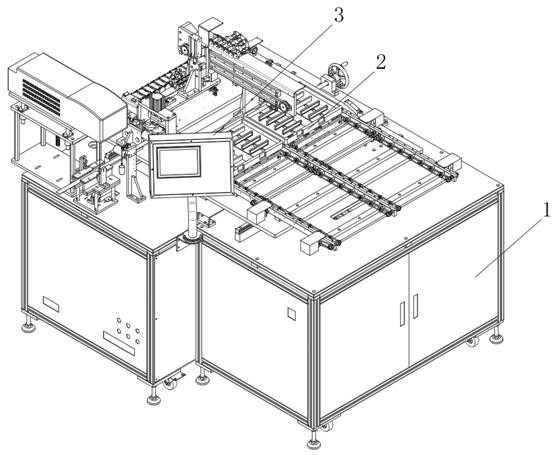
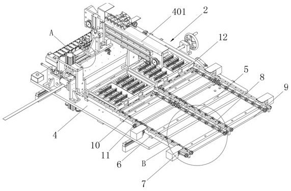
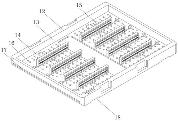
[0048] see Figure 1-11 As shown, a lithography device for a mainboard for semiconductor packaging includes a carrier cabinet 1 and a processing tray 2, and the processing tray 2 is horizontally arranged on the upper end surface of the carrier cabinet 1;

[0049] Wherein, a supporting plate 4 is arranged horizontally at the bottom of the processing tray 2, a photolithography table 401 is arranged above the supporting plate 4, and side mounting plates 6 are arranged at both ends of the supporting plate 4, and the bottoms of ...


PUM


Abstract

Disclosed is a photoetching device of a mainboard for semiconductor packaging. The photoetching device comprises a supporting and mounting cabinet and a processing disc, the processing disc is horizontally arranged on the upper end face of the supporting and mounting cabinet, a supporting plate is horizontally arranged at the bottom of the processing disc, a photoetching table is arranged above the supporting plate, side mounting plates are arranged at the edges of the two ends of the supporting plate, and a plurality of fixing rods are arranged at the bottoms of the two side mounting plates in parallel at equal intervals. The device has the beneficial effects that a top clamping plate is driven by a first hydraulic pump to move up and down, the clamping and fixing position of the mainboard is adjusted, it is guaranteed that the device can conduct top clamping and fixing on mainboards with different widths and lengths, the universality of adaptation is guaranteed, rubber blocks of obtuse triangle structures are attached to the end of the mainboard, the contact area between the rubber blocks and the end part of the mainboard is larger, so that the mainboard is firmer when being photoetched, the mainboard and the top clamping plate are prevented from being scratched and damaged, the photoetched quality of the mainboard is improved, and the service life of each part of the deviceis prolonged.

Description

technical field [0001] The invention relates to a lithography device, in particular to a lithography device for a motherboard for semiconductor packaging and a working method thereof, and belongs to the technical field of application of a lithography device for a semiconductor motherboard. Background technique [0002] The main board is indispensable in semiconductor packaging and processing. The semiconductor components are welded to the main board through packaging, and each semiconductor component works together through the circuit on the main board to ensure the normal operation of the main board. [0003] Before the semiconductor is packaged on the motherboard, a lithography device is required to laser-engrav the surface of the motherboard. On the one hand, the position of the semiconductor package on the motherboard is more accurate and suitable, and on the other hand, the circuit layout on the motherboard is more reasonable. [0004] The patent with publication number...

Claims


Application Information

Patent Timeline
Patent Type & Authority Applications(China)
IPC IPC(8): G03F7/20
CPCG03F7/707G03F7/70716G03F7/70733G03F7/70383G03F7/70908Y02P70/50
Inventor 余中优余杨琴
Owner 上海禾馥电子有限公司
Why Eureka
Try Eureka