Preparation method of thick-film hybrid circuit substrate side resistors

A technology of thick film mixing and substrate side, which is applied in the direction of resistance manufacturing, circuit, resistor, etc., to achieve the effect of wide resistance range, high precision and increased integration density

Inactive Publication Date: 2021-02-02
EAST CHINA INST OF OPTOELECTRONICS INTEGRATEDDEVICE
View PDF7 Cites 4 Cited by
  • Summary
  • Abstract
  • Description
  • Claims
  • Application Information

AI Technical Summary

Problems solved by technology

[0005] Thick film resistors are commonly used in thick film hybrid circuits. If the resistors are connected to the side of the ceramic substrate, it will greatly improve the utilization of integrated space and bring flexibility to the layout design of thick film hybrid circuits. However, there is no related technology at this stage. means

Method used


Image

  • Preparation method of thick-film hybrid circuit substrate side resistors
  • Preparation method of thick-film hybrid circuit substrate side resistors
  • Preparation method of thick-film hybrid circuit substrate side resistors

Examples


Embodiment Construction

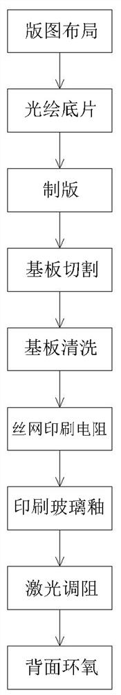
[0023] combine Figure 1~3 As shown, the present invention provides a method for preparing side resistors of a thick-film hybrid circuit substrate, comprising the following steps:

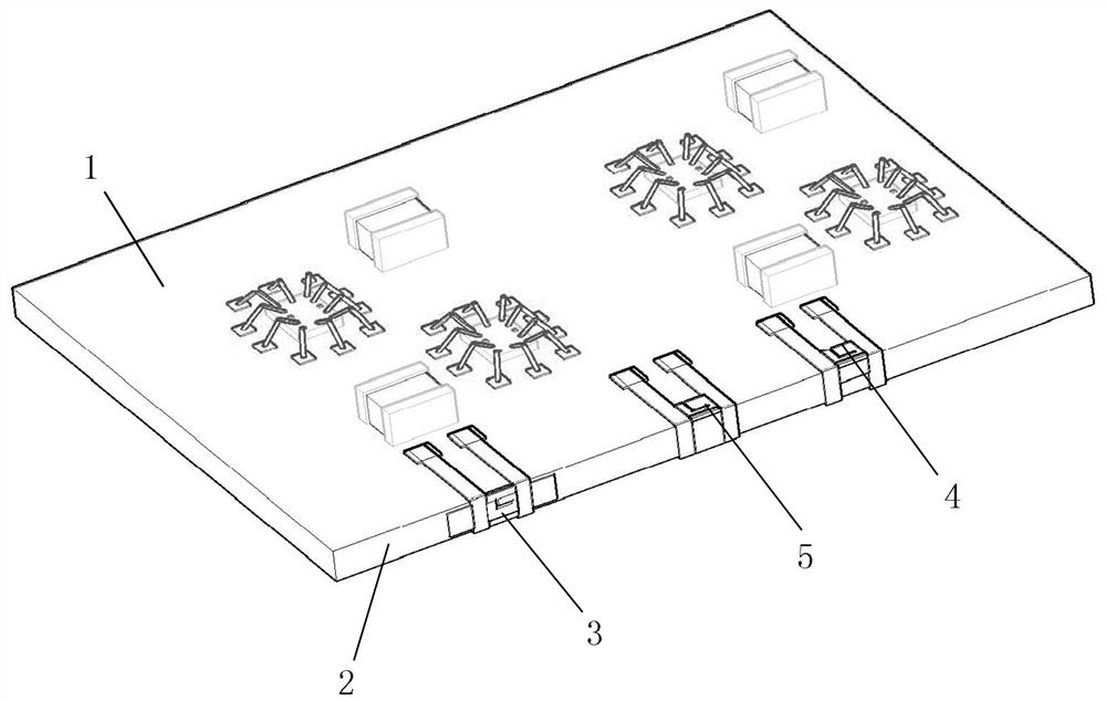
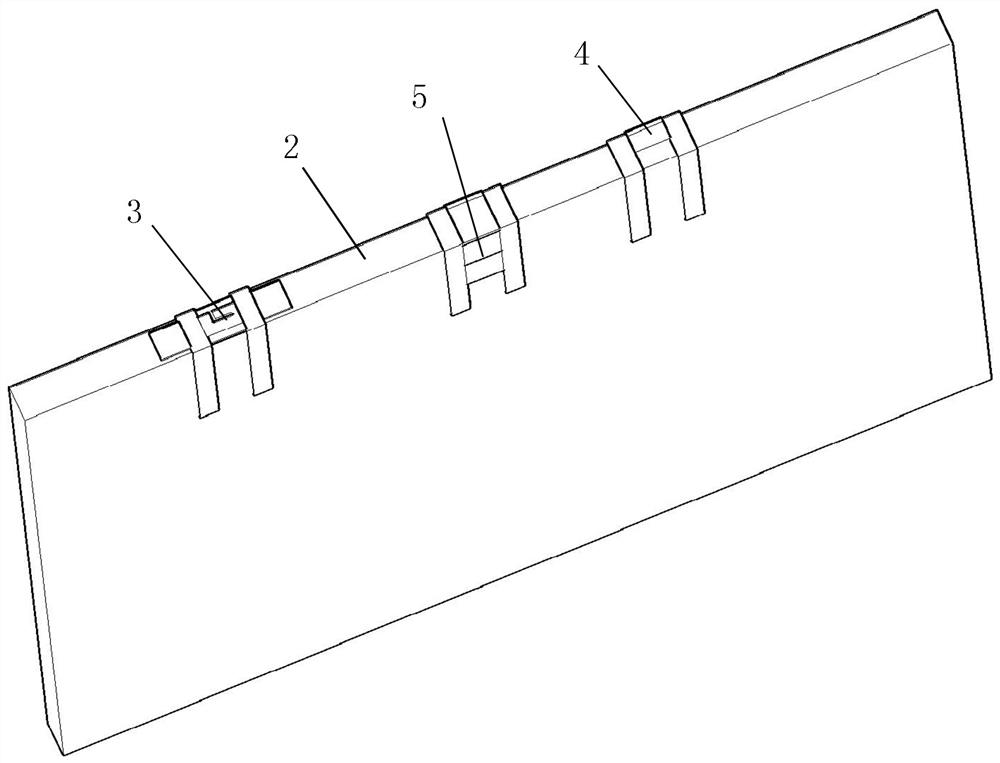
[0024] S1. Carry out the layout layout according to the circuit schematic diagram, determine the resistor positions distributed on the side 2 of the substrate 1, and obtain the resistor layout of the thick film hybrid circuit; there are three types of side resistors, the first type of side resistor 3 is only located on the side of the substrate, and the second type The side resistor 4 spans the side of the substrate and any surface above and below the substrate at the same time, that is, the resistor spans two surfaces; the third type of side resistor 5 spans the side of the substrate and the upper and lower surfaces of the substrate at the same time, that is, the resistor spans three surfaces;

[0025] S2. Light painting negatives, transfer the resistance layout of the thick film hybrid circuit in...


PUM


Abstract

The invention discloses a preparation method of thick-film hybrid circuit substrate side resistors, which comprises the following steps that layout is conducted: three kinds of side resistor are laid,the first side resistor is only positioned on the side surface of a substrate, and the second side resistor simultaneously spans over the side surface of the substrate and any one of the upper surface and the lower surface of the substrate, and the third side resistor simultaneously spans the side surface of the substrate and the upper and lower surfaces of the substrate; a negative film is drawnby light, a plate is made, the substrate is cut and cleaned, and a resistor is printed on the side surface of the substrate by a silk-screen printing process; silk-screen printing of glass glaze on the surface of the printed resistor is conducted; laser resistance trimming is conducted; epoxy insulation treatment is conducted on the back surface of the substrate to obtain the side resistor of thethick-film hybrid circuit substrate. Through the method, the resistor can be manufactured on the side surface of the substrate, the space of the ceramic substrate of the hybrid integrated circuit canbe effectively utilized, the space utilization rate is improved, the integration density is improved, and flexibility is brought to layout design.

Description

technical field [0001] The invention relates to the technical field of thick-film hybrid technology, in particular to a method for preparing side resistors of thick-film hybrid circuit substrates. Background technique [0002] With the miniaturization of thick-film hybrid circuits, the requirements for the integration of internal components are also getting higher and higher. Conventional thick-film hybrid circuits integrate various components, including front integration and back integration of ceramic substrates. At present, the utilization rate of the side of the substrate is low. , such as taking a conventional substrate with a length and width of 30mm×15mm as an example, see Table 1 for the utilization rate under different thicknesses: [0003] Table 1 Utilization of front and back integrated surfaces [0004] Thickness (mm) Front and back area (mm 2 ) Total surface area (mm 2 ) Integrated Utilization 0.50 900 945 95.2% 0.76 900 968....

Claims


Application Information

Patent Timeline
Patent Type & Authority Applications(China)
IPC IPC(8): H01C17/065H05K1/16
CPCH01C17/065H05K1/167
Inventor 李波夏俊生臧子昂李文才符宏大
Owner EAST CHINA INST OF OPTOELECTRONICS INTEGRATEDDEVICE
Why Eureka
Try Eureka