Method for reducing damage to IO interface of packaged chip

A technology for mounting chips and interfaces, applied in the field of reducing damage to the IO interface of packaged chips, can solve the problems of reducing the yield rate of packaged chips, long etching time, and easily damaged IO interfaces of chips, so as to reduce the damage of IO interfaces of chips, improve production efficiency, The effect of accelerating the hole opening efficiency

Pending Publication Date: 2021-02-02
广东佛智芯微电子技术研究有限公司
View PDF3 Cites 2 Cited by
  • Summary
  • Abstract
  • Description
  • Claims
  • Application Information

AI Technical Summary

Problems solved by technology

Among them, when laser drilling is performed on the dielectric layer, the drilling efficiency is high, but it is difficult to accurately control the laser drilling time, and it is easy to damage the IO interface of the chip, thereby reducing the yield of the packaged chip
[0003] Among them, for the laser opening process of the dielectric layer, dry etching can also be used instead, and the exposed holes of the IO interface of the chip are formed by dry etching, but dry etching has the defect of long etching time in the actual operation process, which is serious. Affects the production efficiency of packaged chips

Method used


Image

  • Method for reducing damage to IO interface of packaged chip
  • Method for reducing damage to IO interface of packaged chip
  • Method for reducing damage to IO interface of packaged chip

Examples


Embodiment 1

[0058] Such as figure 1 As shown, in this embodiment, the method for reducing the damage to the IO interface of the packaged chip includes the following steps:

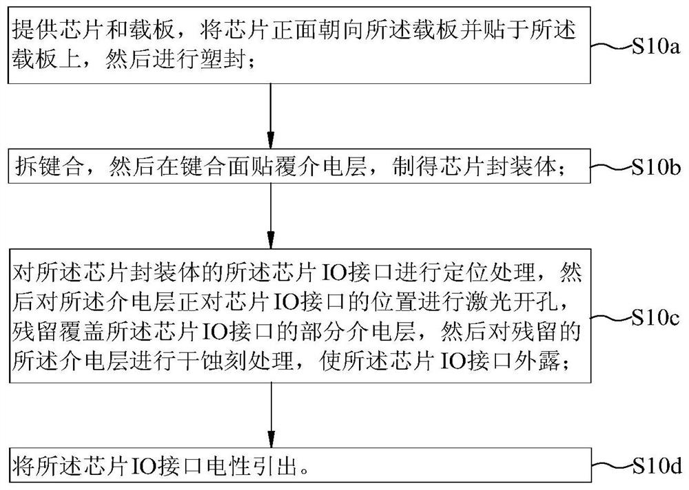
[0059] S10a, providing the chip 2 and the carrier 1, facing the front of the chip 2 to the carrier 1 and pasting it on the carrier 1, and then performing plastic packaging to form a plastic sealing layer 3 covering the chip 2 ( figure 2 );

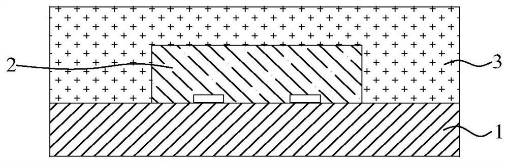
[0060] S10b, dismantling and bonding, turning over, and then sticking a dielectric layer 4 on the bonding surface, making the following image 3 The chip package shown;

[0061] S10c, performing positioning processing on the chip IO interface of the chip package, and then performing laser opening on the position of the dielectric layer 4 facing the chip IO interface ( Figure 4 ), control the laser opening speed and laser opening time, and leave a dielectric layer (residual dielectric layer 41) covering the IO interface of the chip with a thickness of 1-2 μm, and then remove t...

Embodiment 2

[0064] Such as Figure 6 As shown, in this embodiment, the method for reducing the damage to the IO interface of the packaged chip includes the following steps:

[0065] S20a, providing the chip 20 and the carrier 10, the back of the chip 20 faces the carrier 10 and sticks it on the carrier 10, and then performs plastic sealing to form a plastic sealing layer 30 covering the chip 20 ( Figure 7 );

[0066] S20b, performing grinding and thinning treatment on the plastic encapsulation layer 30, and then attaching the dielectric layer 40 to obtain a chip package ( Figure 8 );

[0067] S20c, performing positioning processing on the chip IO interface of the chip package, and then performing laser drilling on the position of the dielectric layer 40 facing the chip IO interface, controlling the laser opening speed and laser opening time, and remaining A dielectric layer (residual dielectric layer 401) covering the IO interface of the chip with a thickness of 1-2 μm ( Figure 9 )...

Embodiment 3

[0070] Such as Figure 11 As shown, in this embodiment, the method for reducing the damage to the IO interface of the packaged chip includes the following steps:

[0071] S30a, providing the chip 200 and the carrier 100, the back of the chip 200 facing the carrier 100 and affixed on the carrier 100, and then performing plastic packaging to form a plastic sealing layer 300 covering the chip 200, and the following is obtained: Figure 12 The chip package shown;

[0072] S30b, performing positioning processing on the chip IO interface of the chip package, and then performing laser opening on the position of the plastic sealing layer 300 facing the chip IO interface, controlling the laser opening speed and laser opening time, and remaining thickness The plastic sealing layer (residual plastic sealing layer 3001) covering the IO interface of the chip is 1-2 μm ( Figure 13 ), and then carry out dry etching treatment on the residual plastic encapsulation layer 3001, so that the IO...


PUM


Abstract

The invention discloses a method for reducing damage to an IO interface of a packaged chip. The method comprises the steps: manufacturing a chip packaging body, sequentially carrying out laser hole forming and dry etching on a position, right opposite to the IO interface of a chip, of the chip packaging body, enabling the IO interface of the chip to be exposed, and then enabling the IO interface of the chip to be electrically led out. According to the invention, the position, right opposite to the chip IO interface, of the chip packaging body is firstly subjected to laser hole forming treatment, and then the residual material covering the chip IO interface is subjected to dry etching treatment, so that the chip IO interface is exposed, the production efficiency of the packaged chip is improved, the damage to the chip IO interface is effectively reduced, and the yield of the packaged chip is improved.

Description

technical field [0001] The invention relates to the technical field of integrated circuit packaging, in particular to a method for reducing damage to an IO interface of a packaged chip. Background technique [0002] The preparation method of the existing chip package structure mainly includes the following steps: making a chip package; providing a dielectric layer, attaching the dielectric layer to the front of the chip package; and performing laser opening treatment on the dielectric layer , forming a window for exposing the chip IO interface of the chip package, and then making a seed layer and a redistribution layer to realize the electrical connection between the chip IO interface and the redistribution layer. Among them, when laser drilling is performed on the dielectric layer, the drilling efficiency is high, but it is difficult to accurately control the laser drilling time, and it is easy to damage the IO interface of the chip, thereby reducing the yield rate of the p...

Claims


Application Information

Patent Timeline
Patent Type & Authority Applications(China)
IPC IPC(8): H01L21/768H01L21/56
CPCH01L21/76805H01L21/568H01L2224/18
Inventor 环珣杨斌
Owner 广东佛智芯微电子技术研究有限公司
Why Eureka
Try Eureka