Optical transceiver circuit and optical transceiver device

An optical transceiver and circuit technology, applied in electromagnetic transceivers and other directions, can solve the problems of high price, difficult to integrate, and large volume, and achieve the effects of low device and assembly cost, small volume, and simple device structure.

Active Publication Date: 2022-06-14
XIAN MICROELECTRONICS TECH INST
View PDF3 Cites 0 Cited by
  • Summary
  • Abstract
  • Description
  • Claims
  • Application Information

AI Technical Summary

Problems solved by technology

[0004] The purpose of the present invention is to overcome the existing high-speed optoelectronic devices / circuits in the above-mentioned prior art, which are incompatible with modern microelectronics technology and hybrid integration technology, resulting in the disadvantages of high price, large volume, and difficulty in integration, and provide an optical transceiver Circuit and Optical Transceiver

Method used


Image

  • Optical transceiver circuit and optical transceiver device
  • Optical transceiver circuit and optical transceiver device
  • Optical transceiver circuit and optical transceiver device

Examples


Embodiment Construction

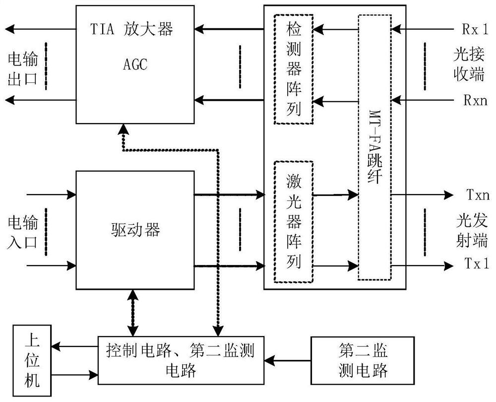
[0035] In order to make those skilled in the art better understand the solutions of the present invention, the technical solutions in the embodiments of the present invention will be clearly and completely described below with reference to the accompanying drawings in the embodiments of the present invention. Obviously, the described embodiments are only Embodiments are part of the present invention, but not all embodiments. Based on the embodiments of the present invention, all other embodiments obtained by persons of ordinary skill in the art without creative efforts shall fall within the protection scope of the present invention.

[0036] It should be noted that the terms "first", "second" and the like in the description and claims of the present invention and the above drawings are used to distinguish similar objects, and are not necessarily used to describe a specific sequence or sequence. It is to be understood that the data so used may be interchanged under appropriate ...


PUM


Abstract

The invention belongs to the field of hybrid integrated optical transceiver design, and discloses an optical transceiver circuit and an optical transceiver device. The optical transceiver circuit includes a driver, a laser array, a detector array, a TIA amplifier, an MT-FA fiber jumper, and a control circuit; the driver is sequentially connected Laser array, MT-FA fiber jumper, detector array and TIA amplifier, optical receiving end and optical transmitting end are set on MT-FA fiber jumper, control circuit is connected with driver and amplifier; optical transceiver device includes optical transceiver circuit, high-speed differential line And a base plate, a base plate, a frame and a cover plate which are sequentially connected from bottom to top. The structure of the device used is simple, and it can be better compatible with modern microelectronics technology and hybrid integration technology. The cost of devices and assembly is low, and the volume is small. It can effectively replace the existing electrical transmission mode and be applied to broadband data in radar and aerospace systems. And image transmission, and then solve the bottleneck problems such as large signal capacity and large data transmission loss in the system.

Description

technical field [0001] The invention belongs to the field of hybrid integrated optical transceiver design, and relates to an optical transceiver circuit and an optical transceiver device. Background technique [0002] With the further development of the information society and the arrival of the era of big data, traditional communication and interconnection technologies are increasingly unable to meet the requirements of data transmission and processing for transmission capacity, communication speed, signal delay, transmission distance and power consumption. Hybrid integrated optoelectronic technology, with its unprecedented technical superiority, provides an ideal way to solve the above problems successfully. It is developing rapidly and will gradually become the main technology for building the key hardware foundation of modern information society. The rapid development of hot industries such as big data and cloud computing urgently requires a large number of cost-effectiv...

Claims


Application Information

Patent Timeline
Patent Type & Authority Patents(China)
IPC IPC(8): H04B10/40
CPCH04B10/40
Inventor 高苏芳朱骏牛士敏陈龙飞徐鑫郑东飞王云
Owner XIAN MICROELECTRONICS TECH INST
Why Eureka
Try Eureka