
Preparation method of high-electron-mobility transistor

A high electron mobility, transistor technology, applied in semiconductor/solid-state device manufacturing, circuits, electrical components, etc., can solve problems such as easy formation of leakage channels and poor antistatic ability of HEMT

Active Publication Date: 2021-02-12
HC SEMITEK ZHEJIANG CO LTD
View PDF4 Cites 0 Cited by
  • Summary
  • Abstract
  • Description
  • Claims
  • Application Information

AI Technical Summary

Problems solved by technology

[0004] There are a lot of dislocations and defects in the GaN channel layer grown on the Si substrate, which is easy to form leakage channels, resulting in poor antistatic ability of HEMT

Method used


Image

  • Preparation method of high-electron-mobility transistor
  • Preparation method of high-electron-mobility transistor
  • Preparation method of high-electron-mobility transistor

Examples


Embodiment Construction

[0033] In order to make the purpose, technical solution and advantages of the present disclosure clearer, the implementation manners of the present disclosure will be further described in detail below in conjunction with the accompanying drawings.

[0034] The epitaxial structure of the HEMT includes a substrate, a channel layer and a barrier layer, and the channel layer and the barrier layer are sequentially stacked on the substrate. The substrate acts as a support and provides a surface for epitaxial growth; the channel layer and the barrier layer are formed of different materials, and a two-dimensional electron gas with high concentration and high mobility is formed at the heterojunction interface.

[0035] Both the sapphire substrate and the Si substrate are relatively cheap and suitable for industrial production. Compared with sapphire substrates, which have the characteristics of high hardness, poor thermal conductivity, and insulation, Si substrates have the advantages ...


PUM

PropertyMeasurementUnit
thicknessaaaaaaaaaa
thicknessaaaaaaaaaa
thicknessaaaaaaaaaa

Abstract

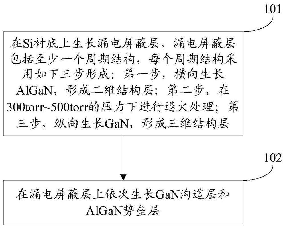
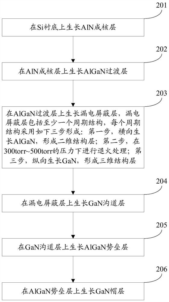
The invention provides a preparation method of a high-electron-mobility transistor, which belongs to the technical field of semiconductors. The preparation method comprises the steps that an electricleakage shielding layer grows on a Si substrate, the electric leakage shielding layer comprises at least one periodic structure, and each periodic structure is formed through the following three stepsoft firstly, transversely growing AlGaN to form a two-dimensional structure layer, secondly, conducting annealing treatment under the pressure of 300 torr to 500 torr, and thirdly, longitudinally growing GaN to form a three-dimensional structure layer. Sequentially, a GaN channel layer and an AlGaN barrier layer grow on the electric leakage shielding layer. The electric leakage shielding layer comprising at least one periodic structure grows on the Si substrate, the epitaxial defect density can be reduced to 106 / cm<2> or below, formation of an electric leakage channel is effectively inhibited, the probability of tunnel breakdown of the HEMT is reduced, the antistatic capacity of the HEMT is improved, and the reliability of the HEMT is ensured to meet the requirement.

Description

technical field [0001] The present disclosure relates to the technical field of semiconductors, in particular to a preparation method of a high electron mobility transistor. Background technique [0002] HEMT (High Electron Mobility Transistor, High Electron Mobility Transistor) is a type of FET (Field Effect Transistor, Field Effect Transistor), which uses two materials with different energy gaps to form a heterojunction to provide a channel for carriers. [0003] In the related art, the HEMT includes an epitaxial structure and a source, a drain, and a gate respectively arranged on the epitaxial structure. The source and the drain form an ohmic contact with the epitaxial structure, and a Schottky contact is formed between the gate and the epitaxial structure. touch. The epitaxial structure includes a Si substrate and a GaN channel layer and an AlGaN barrier layer stacked on the Si substrate in sequence. The Si substrate plays a supporting role and provides a surface for ep...

Claims


Application Information

Patent Timeline
Patent Type & Authority Applications(China)
IPC IPC(8): H01L21/335H01L29/06
CPCH01L29/66462H01L29/0607
Inventor 洪威威王倩梅劲董彬忠胡加辉
Owner HC SEMITEK ZHEJIANG CO LTD
Learn More