light emitting device
A light-emitting device and packaging layer technology, applied in semiconductor devices, electrical components, circuits, etc., can solve the problems of large package structure, increased package thickness, and high cost of quartz glass, so as to improve transmittance, reduce product size, cost reduction effect
- Summary
- Abstract
- Description
- Claims
- Application Information
AI Technical Summary
Problems solved by technology
Method used
Image
Examples
Embodiment 1
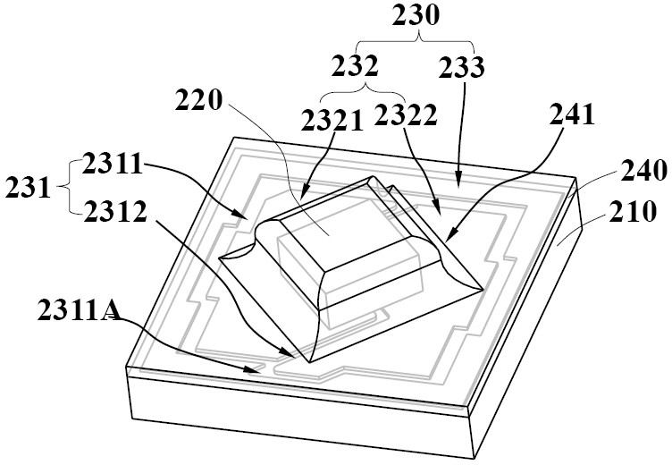
[0040] Please see attached figure 2 , this embodiment discloses an ultraviolet packaging device, including: a packaging substrate 210, a patterned conductive layer 230 located on the upper surface of the substrate, an LED chip disposed on the substrate 210 and electrically connected to the conductive layer 230 220, and the encapsulation layer 240 covering the upper surface of the substrate and the LED chip 220, the encapsulation layer 240 forms an optical structure at the position corresponding to the LED chip 220, and the optical structure has a curved surface above the LED chip and / or on the side wall, which can be adjusted Lighting angle and spatial distribution of light intensity of the device.
[0041] Specifically, the substrate 210 includes an upper surface and a lower surface, and the substrate 210 may be made of materials commonly used in the field, such as ceramics or silicon, preferably a ceramic substrate. The size of the substrate can be selected according to re...
Embodiment 2
[0056] Figure 7 A light emitting device embodied in accordance with the present invention is shown. exist Figure 4 In the light-emitting device shown, the thickness of the LED chip is more than 300 μm, and the thickness T of the encapsulation layer 240 30 Less than the thickness of the LED chip, in the light emitting device shown in this embodiment, the thickness T of the LED chip 20 is less than 300 μm, for example, 150 μm to 200 μm, or 200 μm to 300 μm, the first thickness T of the encapsulation layer 240 31 with the thickness T of the LED chip 220 20 The relationship is preferably 1.2T 20 ≥T 31 ≥0.5T 20 , at this time, the encapsulation layer 240 can better cover the LED chip 240, and form an optical structure with a curved surface on the LED chip, such as T 31 ≈T 20 . Further, 0μm≤T 31 -T 32 ≤50 μm, that is, the thickness of the encapsulation layer 240 on the upper surface of the LED chip is relatively uniform. Further, the thickness of the encapsulation lay...
Embodiment 3
[0060] Figure 8 A light emitting device embodied in accordance with the present invention is shown. In this embodiment, on the basis of Embodiment 1, a series of additional grooves 2313 are arranged on the edge region 233 of the patterned conductive layer 230 on the substrate. The depth of the series of additional grooves 2313 is preferably half the thickness of the patterned conductive layer. Above, it can also be greater than or equal to the thickness of the conductive layer 230 , and the encapsulation layer 240 fills the series of additional grooves 2313 , thereby increasing the bonding force between the encapsulation layer 240 and the substrate 210 .
PUM
| Property | Measurement | Unit |
|---|---|---|
| thickness | aaaaa | aaaaa |
| thickness | aaaaa | aaaaa |
| thickness | aaaaa | aaaaa |
Abstract
Description
Claims
Application Information


