Stacked shielded inductor

A layered and inductive technology, applied in the direction of inductors, printed inductors, fixed inductors, etc., can solve problems such as circuit system interference, narrow channels, and affecting circuit system reliability, and achieve reduced external radiation and high Q value , The effect of small coupling interference voltage

Inactive Publication Date: 2021-02-23
SHENZHEN SUNLORD ELECTRONICS
View PDF1 Cites 1 Cited by
  • Summary
  • Abstract
  • Description
  • Claims
  • Application Information

AI Technical Summary

Problems solved by technology

[0002] With the development of communication technologies such as WiFi6 and 5G, the application frequency is getting higher and higher, and the channel is getting narrower and narrower. As a radiation source, the inductance device needs to consider EMI during the application process. The external radiation of the inductance device is likely to cause damage to the circuit system, especially The interference of the sensitive circuit affects the reliability of the circuit system

Method used


Image

  • Stacked shielded inductor
  • Stacked shielded inductor
  • Stacked shielded inductor

Examples


Embodiment Construction

[0026] Embodiments of the present invention will be described in detail below. It should be emphasized that the following description is only exemplary and not intended to limit the scope of the invention and its application.

[0027] It should be noted that when an element is referred to as being “fixed” or “disposed on” another element, it may be directly on the other element or be indirectly on the other element. When an element is referred to as being "connected to" another element, it can be directly connected to the other element or indirectly connected to the other element. In addition, the connection can be used for fixation as well as for coupling or communication.

[0028] It is to be understood that the terms "length", "width", "top", "bottom", "front", "rear", "left", "right", "vertical", "horizontal", "top" , "bottom", "inner", "outer" and other indicated orientations or positional relationships are based on the orientations or positional relationships shown in ...


PUM


Abstract

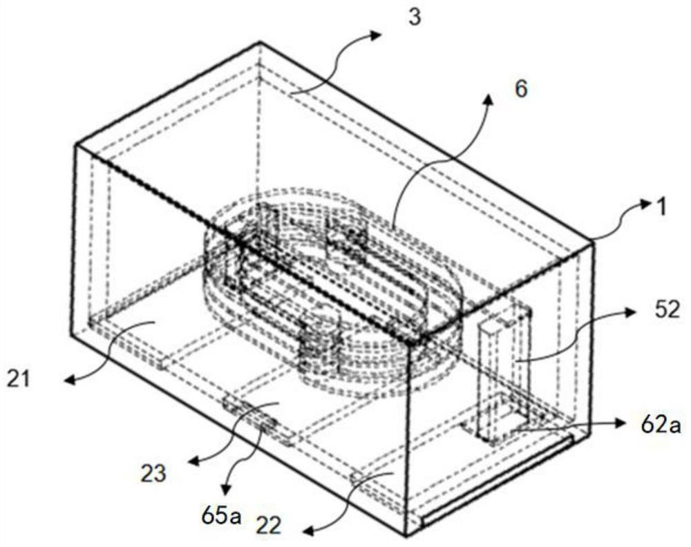
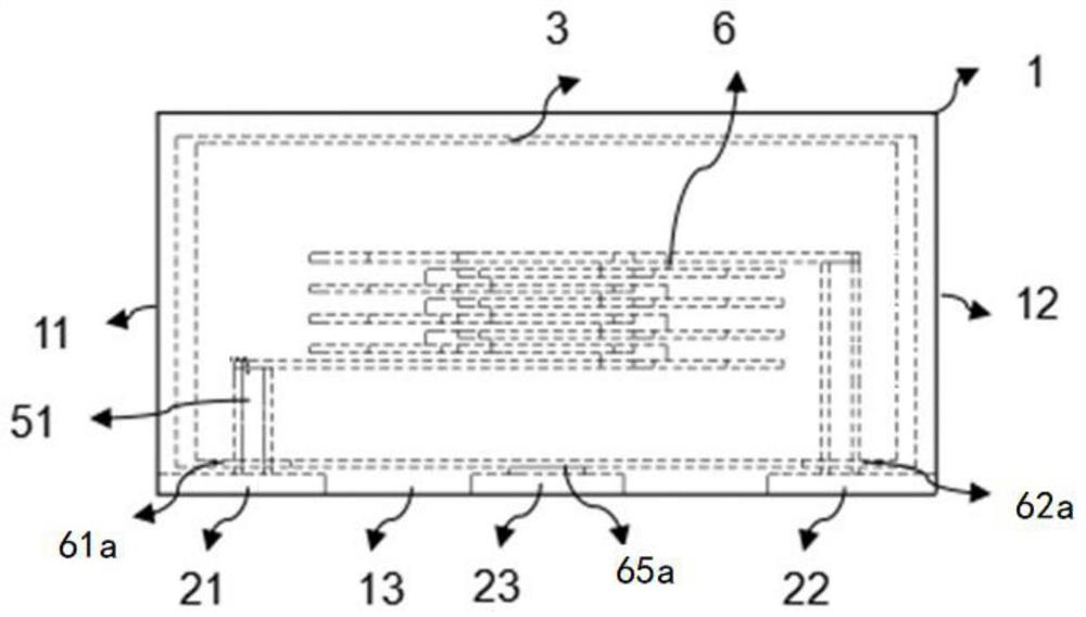
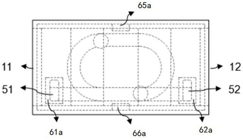
A stacked shielded inductor, comprising a stacked body, an internal wire coil, a first external electrode, a second external electrode, a third external electrode, and a shielding cover. The stacked body comprises a plurality of insulating body layers arranged in a stacked manner, and shielding conductor channels positioned on the periphery of the internal wire coil is opened in the plurality of insulating body layers. Each shielding conductor channel is internally provided with a shielding conductor, and the channels are electrically connected to one another, together forming a shielding conductor stacking layers surrounding the outside of the internal wire coil. A shielding conductor upper layer and a shielding conductor lower layer are respectively arranged above and below the internalwire coil, the shielding conductor stacking layers, the shielding conductor upper layer, and the shielding conductor lower layer closing to form a shielding cover that encloses the internal wire coil,the shielding cover being connected to the third external electrode arranged on a surface of the stacked body. Thus, the present invention is able to achieve a high screening effect for a stacked surface-mounted inductor, effectively reducing outward radiation from the stacked surface-mounted inductor, and thereby improving the reliability of a circuit system.

Description

technical field [0001] The invention relates to a laminated electronic device, in particular to a laminated shielded inductor. Background technique [0002] With the development of communication technologies such as WiFi6 and 5G, the application frequency is getting higher and higher, and the channel is getting narrower and narrower. As a radiation source, the inductance device needs to consider EMI during the application process. The external radiation of the inductance device is likely to cause damage to the circuit system, especially The interference of the sensitive circuit affects the reliability of the circuit system. [0003] The disclosure of the above background technical content is only used to assist in understanding the inventive concepts and technical solutions of the present invention, and it does not necessarily belong to the prior art of this patent application. There is no clear evidence that the above content has been disclosed on the filing date of this pa...

Claims


Application Information

Patent Timeline
Patent Type & Authority Applications(China)
IPC IPC(8): H01F27/36H01F27/28
CPCH01F27/2804H01F2027/2809H01F17/0013H01F2017/008H01F27/292H01F27/2885H01F27/324
Inventor 杨翌华陈先仁吴中东
Owner SHENZHEN SUNLORD ELECTRONICS
Why Eureka
Try Eureka