Method of determining OPC minimum segmentation length
A minimum and wide technology, applied in the photoplate making process of the pattern surface, the original for photomechanical processing, the microlithography exposure equipment, etc., can solve the problem of low OPC correction accuracy, and the target layout pattern cannot be reasonably segmented, etc. problems, to achieve the effect of improving product yield
- Summary
- Abstract
- Description
- Claims
- Application Information
AI Technical Summary
Problems solved by technology
Method used
Image
Examples
Embodiment 1
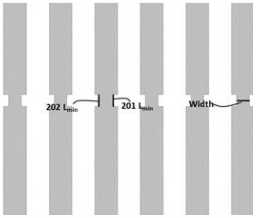
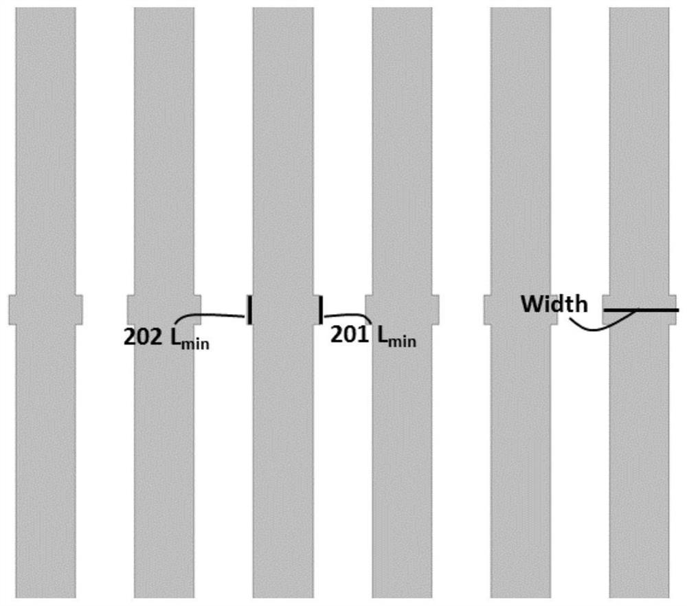
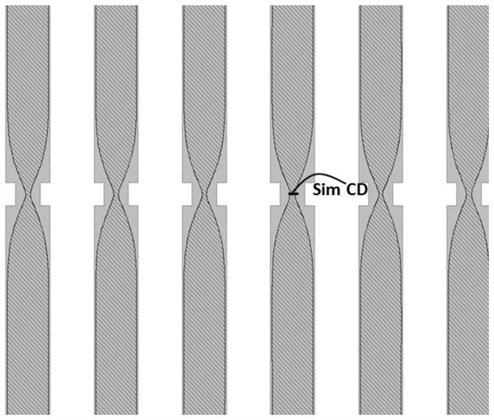
[0040] The present invention provides a method for determining the OPC minimum segment length, such as Figure 7 as shown, Figure 7 Shown is the flow chart of the method for determining the OPC minimum segment length of the present invention. The method at least includes the following steps:
[0041] Step 1. Determine the target layer and the ADI target value corresponding to the target layer (CD of the photoresist pattern after development) as ADItarget; further in the present invention, the ADI target value in step 1 of this embodiment is the graphic line width (The line width of the photoresist pattern after development). Still further in the present invention, the ADI target value ADI target in step 1 of this embodiment is 81nm.
[0042] Step 2, obtain the value range and the value range of the length segment value and the width or spacing segment value based on the OPC-processed test pattern according to the ADI target value; within the value range of the length segme...
Embodiment 2
[0050] The present invention provides a method for determining the OPC minimum segment length, such as Figure 7 as shown, Figure 7 Shown is the flow chart of the method for determining the OPC minimum segment length of the present invention. The method at least includes the following steps:
[0051] Step 1. Determine the target layer and the ADI target value corresponding to the target layer (CD of the photoresist pattern after development) as ADItarget; further in the present invention, the ADI target value in step 1 of this embodiment is the pattern pitch ( The distance between two adjacent photoresist patterns after development) Further in the present invention, the ADI target value ADItarget in step 1 of this embodiment is 81 nm.
PUM
 Abstract
Description
Claims
Application Information


