Manufacturing method of display panel, display panel and display device
A technology for display panels and manufacturing methods, applied in semiconductor/solid-state device manufacturing, electrical components, electric solid-state devices, etc., can solve problems such as color mixing, mura brightness, unevenness, etc., to reduce the probability of color mixing and mura phenomena, and prevent The effect of overflowing pixel pits
- Summary
- Abstract
- Description
- Claims
- Application Information
AI Technical Summary
Problems solved by technology
Method used
Image

Examples
Embodiment 1
[0035] At present, the mature display technology on the market is LCD (liquid crystal display) technology, while new display technologies such as OLED (organic electroluminescence display) and QLED (quantum dot electroluminescence display) use self-luminescence to bring high contrast and high color. Wide field of view, wide viewing angle, low energy consumption, low response time, and its advantages of being lighter and thinner have attracted everyone's attention.
[0036] At present, display giants such as Samsung and LG have launched large-size OLED TV products, and even OLED TV products with curved screens are available. However, due to the high cost of large-size OLED products, the mass-produced OLED displays on the market are still mainly small-sized, and the number of large-sized OLEDs is small. Facing the cruel market environment, it is difficult to form a competitive advantage. The main factor limiting large-size OLED displays is the fabrication of OLED devices. At pr...
Embodiment 2
[0046] In order to better describe the manufacturing method of the display panel in the first embodiment, this embodiment specifically describes the manufacturing method of the display panel on the basis of the above-mentioned embodiments.
[0047] See Figure 2a-Figure 2f , Figure 2a-Figure 2f It is a schematic diagram of a method for manufacturing a display panel provided by an embodiment of the present invention. The manufacturing method of the display panel may specifically include:
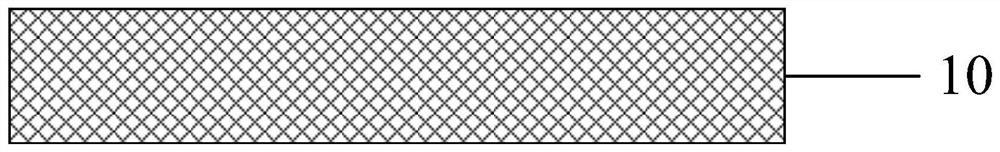
[0048] Step 1. Provide a base substrate 10. The base substrate 10 is a TFT substrate. The TFT substrate may specifically include a glass substrate, a TFT array layer, a planarization layer covering the TFT array layer, and a plurality of pixels arranged on the planarization layer. A plurality of anodes corresponding to the region, the TFT array layer can specifically include a plurality of TFTs (Thin Film Transistor, thin film transistors), scanning signal lines (or gate lines) for transmi...
Embodiment 3
[0070] This embodiment also provides a display panel on the basis of the above embodiments, the display panel is manufactured according to the manufacturing method of any one of the above embodiments, please refer to image 3 , the display panel may specifically include a base substrate 10, a final photoresist layer having pixel pits 50, and a color resist layer 70, wherein:
[0071] The base substrate 10 is a TFT substrate, and the TFT substrate may specifically include a glass substrate, a TFT array layer, a planarization layer covering the TFT array layer, and a plurality of anodes disposed on the planarization layer corresponding to a plurality of pixel regions.
[0072] The final photoresist layer is located on the base substrate 10, and the material of the final photoresist layer is a negative photoresist material mixed with photosensitive materials, and the final photoresist layer includes a first photoresist layer and a photoresist layer located on the first photoresist...
PUM
| Property | Measurement | Unit |
|---|---|---|
| thickness | aaaaa | aaaaa |
Abstract
Description
Claims
Application Information
 - R&D
- Intellectual Property
- Life Sciences
- Materials
- Tech Scout
- Unparalleled Data Quality
- Higher Quality Content
- 60% Fewer Hallucinations
Browse by: Latest US Patents, China's latest patents, Technical Efficacy Thesaurus, Application Domain, Technology Topic, Popular Technical Reports.
© 2025 PatSnap. All rights reserved.Legal|Privacy policy|Modern Slavery Act Transparency Statement|Sitemap|About US| Contact US: help@patsnap.com