
Image sensor

An image sensor and pixel technology, applied in the field of image sensors, can solve the problems of optical crosstalk, reduced chip space utilization, cost increase, etc., to achieve the effect of reducing costs and improving space utilization

Pending Publication Date: 2021-02-26
GALAXYCORE SHANGHAI
View PDF10 Cites 0 Cited by
  • Summary
  • Abstract
  • Description
  • Claims
  • Application Information

AI Technical Summary

Problems solved by technology

[0006] However, in some existing image sensors, in order to avoid the problem of optical path crosstalk that easily occurs when one microlens corresponds to multiple pixel units, resulting in blurred imaging, redundant areas are added to form redundant (Dummy) pixel units (Pixel Cell), leading to a reduction in the space utilization of the chip and an increase in cost

Method used


Image

  • Image sensor
  • Image sensor
  • Image sensor

Examples


Embodiment Construction

[0033] As mentioned above, an existing image sensor includes a pixel unit array and peripheral circuits, wherein the peripheral circuits may include row driver circuits, column readout circuits, digital processing circuits, and other peripheral circuits. However, , in order to avoid blurred imaging due to the problem of optical path crosstalk when one microlens corresponds to multiple pixel units, redundant areas will be added to form redundant pixel units, resulting in reduced space utilization of the chip and increased cost.

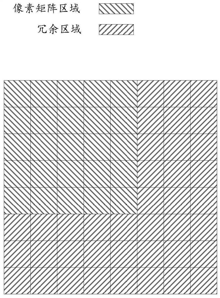
[0034] refer to figure 1 , figure 1 It is a schematic top view of a device cross-sectional structure of an image sensor in the prior art.

[0035] Such as figure 1 As shown, the pixel unit array can be divided into several pixel unit sub-arrays, wherein the pixel unit sub-array is divided into a pixel matrix area with effective pixels and a redundant area, wherein the pixel matrix Regions can have a matrix of pixels.

[0036] It should be pointed o...


PUM


Abstract

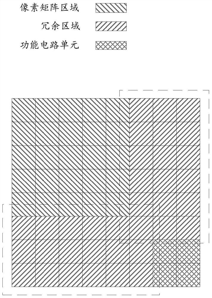
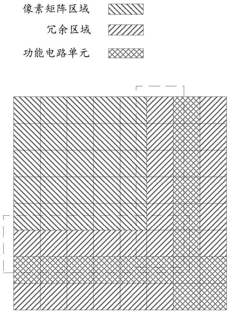
An image sensor comprises a pixel unit array, the pixel unit array is divided into a plurality of pixel unit sub-arrays, and the pixel unit sub-arrays are divided into pixel matrix areas with effective pixels and redundant areas; each redundant region has one or more functional circuit units for implementing one or more electronic circuit functions, and comprises at least a part of the circuit module and / or electronic components. According to the invention, the space utilization rate of the chip can be effectively improved, and the cost can be reduced.

Description

technical field [0001] The invention relates to the field of integrated circuits, in particular to an image sensor. Background technique [0002] Image sensors have been used in various fields such as machine vision, robotics, satellite-based instruments, transportation, navigation and guidance. Typically, an image sensor has a two-dimensional array of pixels that make up an image frame. [0003] Among them, a pixel includes a photoelectric conversion element capable of accumulating charges corresponding to the amount of absorbed light. In other words, when photons collide with the surface of the photoelectric conversion element formed on the semiconductor substrate, free carriers are generated and collected in the photoelectric conversion element. The collected carriers are read out and then transferred to an output circuit through various processes, thereby reproducing an image. [0004] An existing image sensor includes a pixel unit array (pixel array) and peripheral c...

Claims


Application Information

Patent Timeline
Patent Type & Authority Applications(China)
IPC IPC(8): H04N5/378H04N5/369
CPCH04N25/70H04N25/75
Inventor 赵立新李怀兆
Owner GALAXYCORE SHANGHAI
Learn More