
A Method of Mosfet Gate-Source Voltage Response to High-frequency Pulse Interference

A gate-source voltage and high-frequency pulse technology, which is applied in the field of MOSFET gate-source voltage response to high-frequency pulse interference, can solve the problems of lack of explanation for interference oscillation, reduce SiC MOSFET gate voltage stress, and difficult to directly face engineering applications, etc., to achieve physical significance Intuitive, improve design efficiency, simple representation effect

Active Publication Date: 2021-10-08
BEIJING JIAOTONG UNIV +1
View PDF4 Cites 0 Cited by
  • Summary
  • Abstract
  • Description
  • Claims
  • Application Information

AI Technical Summary

Problems solved by technology

However, these complex mechanism models only consider the voltage spikes caused by disturbances, and lack explanations for disturbance oscillations; moreover, in the modeling process, too many non-dominant stray parameters are introduced
Therefore, using these complex mechanism models, it is still difficult to directly face engineering applications and give design guidelines considering gate pressure stress; the method of reducing SiC MOSFET gate pressure stress has not yet been fully integrated into the design of high-power converter systems

Method used


Image

  • A Method of Mosfet Gate-Source Voltage Response to High-frequency Pulse Interference
  • A Method of Mosfet Gate-Source Voltage Response to High-frequency Pulse Interference
  • A Method of Mosfet Gate-Source Voltage Response to High-frequency Pulse Interference

Examples


Embodiment Construction

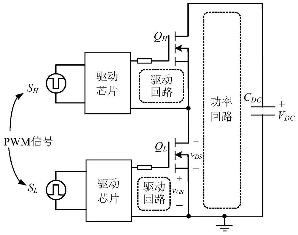
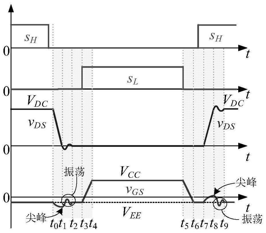
[0048] The present invention respectively establishes a power loop model and a drive loop model, uses a time-domain characteristic method and a frequency-domain characteristic method to describe the dynamic process of the gate-source voltage responding to a high-speed switching interference source, and reveals the coupling induction mechanism of the gate-source voltage oscillation. The method for responding the gate-source voltage of MOSFET to high-frequency pulse interference of the present invention can effectively predict the disturbance peak and disturbance oscillation after the gate-source voltage is disturbed. The embodiments described below by referring to the figures are exemplary and are intended to explain the present invention and should not be construed as limiting the present invention.

[0049] A method for MOSFET gate-source voltage response to high-frequency pulse interference according to an embodiment of the present invention will be described below with refer...


PUM


Abstract

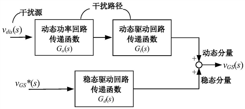
The invention provides a method for MOSFET gate-source voltage response to high-frequency pulse interference, which divides the disturbed gate-source voltage into disturbance dynamic components and steady-state components; establishes a dynamic response model of gate-source voltage according to the disturbance dynamic components and steady-state components , which is used to predict the disturbance spikes and oscillations of MOSFET gate-source voltage in high-frequency high-power converters. It has concise mathematical representation and intuitive physical meaning.

Description

technical field [0001] The invention relates to a method for MOSFET grid-source voltage response to high-frequency pulse interference. Background technique [0002] With the advancement of material technology, power MOSFETs made of wide bandgap semiconductor materials such as SiC and GaN have the advantages of high withstand voltage and fast switching speed. However, this advantage forces the rate of change of drain-source voltage and current to become faster High, seriously affecting the stability of the gate-source voltage. When a power metal oxide semiconductor field effect transistor (MOSFET) is in use, the drastic change of the drain-source voltage and current is reflected by the Miller capacitance, causing the gate-source voltage to be disturbed and appearing spikes and oscillations, affecting the stability of the gate-source voltage and reducing the life of the MOSFET It even directly causes MOSFET failure, seriously restricts the performance improvement of power ele...

Claims


Application Information

Patent Timeline
Patent Type & Authority Patents(China)
IPC IPC(8): G06F30/20G06F30/30G06F17/15
CPCG06F17/15G06F30/20G06F30/30
Inventor 邵天骢郑琼林李志君李虹黄波邱志东张志朋王作兴王佳信
Owner BEIJING JIAOTONG UNIV
Learn More