
Electrical contacting and method for producing an electrical contacting

A technology of electrical contacts and contacts, which is applied in the manufacture of microstructure devices, circuits, electrical components, etc., can solve problems such as high resistance, and achieve the effects of high conductivity, low cost, and small process consumption

Pending Publication Date: 2021-03-02
ROBERT BOSCH GMBH
View PDF4 Cites 0 Cited by
  • Summary
  • Abstract
  • Description
  • Claims
  • Application Information

AI Technical Summary

Problems solved by technology

However, such TSVs have relatively high resistance

Method used


Image

  • Electrical contacting and method for producing an electrical contacting
  • Electrical contacting and method for producing an electrical contacting
  • Electrical contacting and method for producing an electrical contacting

Examples


Embodiment Construction

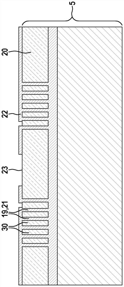
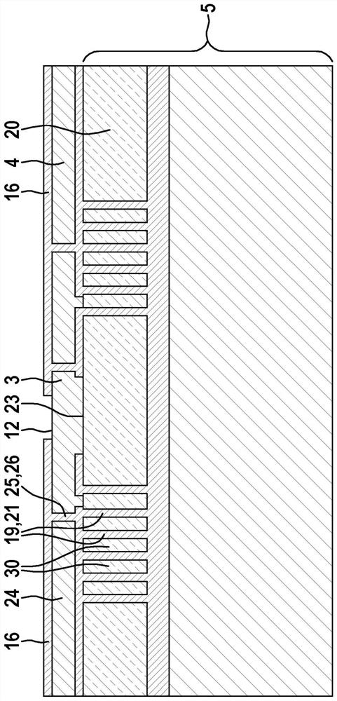
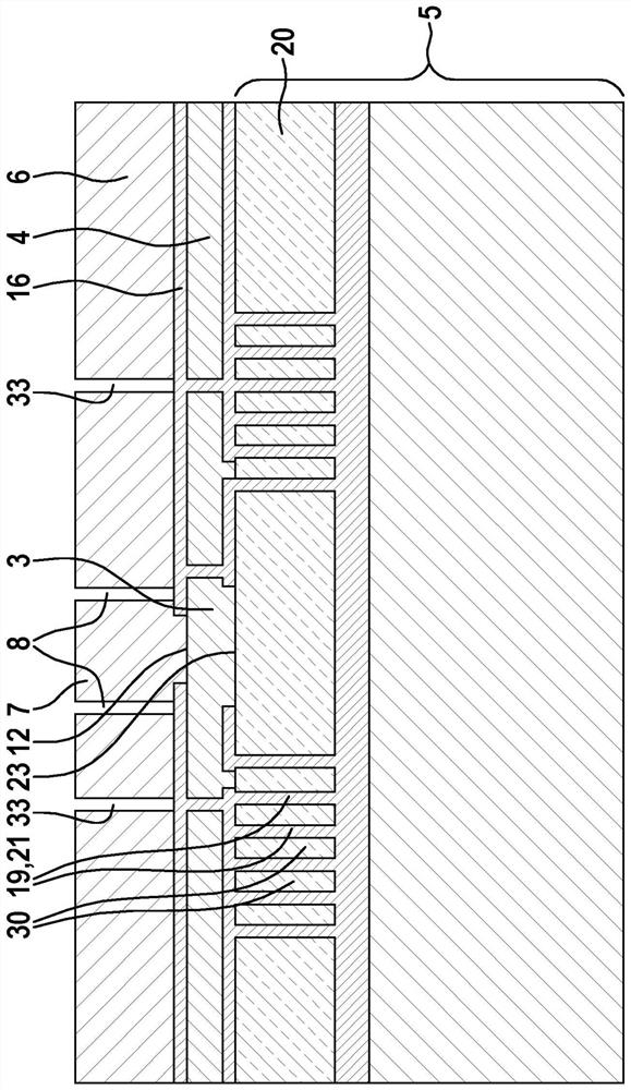
[0050] exist figure 1 A schematic illustration of the method for producing an electrical contact 1 according to an embodiment of the invention after the third preliminary step is shown in . Structures 19 have already been created (dug out) in the silicon layer 20 of the SOI wafer 5 or SOI chip 5 before the second preliminary step. The individual components of the microelectromechanical component 30 are delimited by means of the structure 19 . In a second preliminary step a third insulator 21 has already been deposited in the structure 19 and at the same time a third insulator layer 22 is formed over the silicon layer 20 . Preferably, the third insulator layer 22 and the third insulator 21 respectively consist of the same oxide. In a third pre-step, the insulator layer 22 has been removed in the second contact region 23 .

[0051] exist figure 2 A schematic illustration of the method for producing an electrical contact 1 according to an embodiment of the invention after th...


PUM


Abstract

An electrical contacting (1) between a surrounding wiring (2) and a conductor region (3), wherein the conductor region (3) is arranged in a conductor layer (4) above an SOI wafer (5) or SOI chip (5),wherein a cover layer (6) is arranged above the conductor layer (4) and below the surrounding wiring (2), characterized in that the cover layer (6) has a contacting region (7), wherein the contactingregion (7) is isolated from the rest of the cover layer (6) by means of a first recess arrangement (8), wherein an opening (9) is formed at least in the contacting region (7), wherein a metallic material (10) is arranged in the opening (9), the metallic material (10) connecting the surrounding wiring (2) and the conductor region (3).

Description

technical field [0001] The invention relates to an electrical contact between a rewiring and a conductor region, wherein the conductor region is arranged in a conductor layer above an SOI wafer or SOI chip, wherein a cover layer is arranged above the conductor layer and below the rewiring . Furthermore, the invention relates to a method for producing an electrical contact and a system comprising an electrical contact. Background technique [0002] Electrical contacts are generally known, especially through silicon vias (TSVs). Such a contact can pass through the wafer or only a partial area of ​​the wafer. Typically an attempt is made to achieve the smallest possible feedthroughs while simultaneously achieving low via resistances. To achieve this, elongated holes with approximately vertical walls are often produced in the wafer, for example by means of a trench process or a laser. Insulation is then deposited into the holes. Contact etching takes place through the insul...

Claims


Application Information

Patent Timeline
Patent Type & Authority Applications(China)
IPC IPC(8): B81B7/00
CPCB81B7/007B81B2207/095B81B2207/092B81C1/00301
Inventor T·沙里J·赖因穆特S·马约尼M·库恩克
Owner ROBERT BOSCH GMBH
Learn More